- Products & Capabilities

- About
- Resources
Stencil Printing vs. Jet Printing in PCB Assembly


Compare stencil printing vs jet printing for SMT PCB assembly and learn key differences, pros, cons & pick the best method for your production needs.
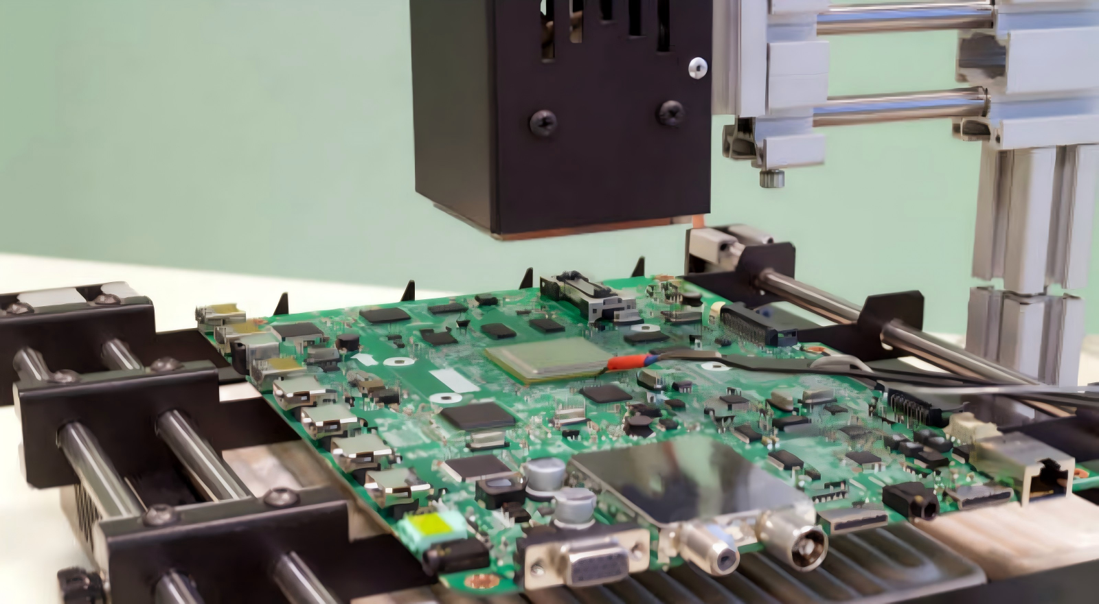
When it comes to surface‑mount technology (SMT) assembly of printed circuit boards (PCBs), the application of solder paste is the key to ensuring good soldering, high yield, and reliable assembly. Research reveals that over 60% of typical SMT problems, such as bridging, insufficient solder, and tombstoning, result from unreliable and/or inaccurate paste deposition. There are two major technologies used: conventional stencil printing and cutting‑edge digital jet printing. Both technologies differ in their operating principles, cost, accuracy and applications. For electronics engineers, contract manufacturing houses, and product designers, selection of the best method depends on production volume, design complexity, cost, and time‑to‑market requirements.
What Is Stencil Printing?
Solder paste stencil printing is the most common method for applying solder paste for medium‑to‑high‑volume PCB production. It involves a precisely etched metal (usually stainless steel) stencil with holes that align to the PCB's pad pattern. In practice, the stencil is positioned on the PCB, and a squeegee is drawn across the stencil at a specified speed and pressure, depositing solder paste through the stencil to the PCB pads. After removing the stencil, the paste remains on the board.
Key Advantages
Fast Turnaround: Cycle times of less than 30 seconds per board enable processing of 100-200 boards per hour in fully automatic lines.
Low Costs for High Volume: After one‑time stencil tooling ($50-500), the per‑unit cost is low, suitable for high volume manufacturing.
High Accuracy: Today's technology offers deposition accuracy of ±25 microns, enabling fine‑pitch components as small as 0.4 mm.
Mature Process: Excellent equipment support, process standardisation and minimal maintenance
Limitations
Rigid Design: PCB design changes require a new stencil, adding cost and lead time.
Paste Amount: No way to fine‑tune paste volume without costly stepped stencils.
Tooling Lead Time: Stencil turn times are 1-3 days, impacting rapid turnaround.
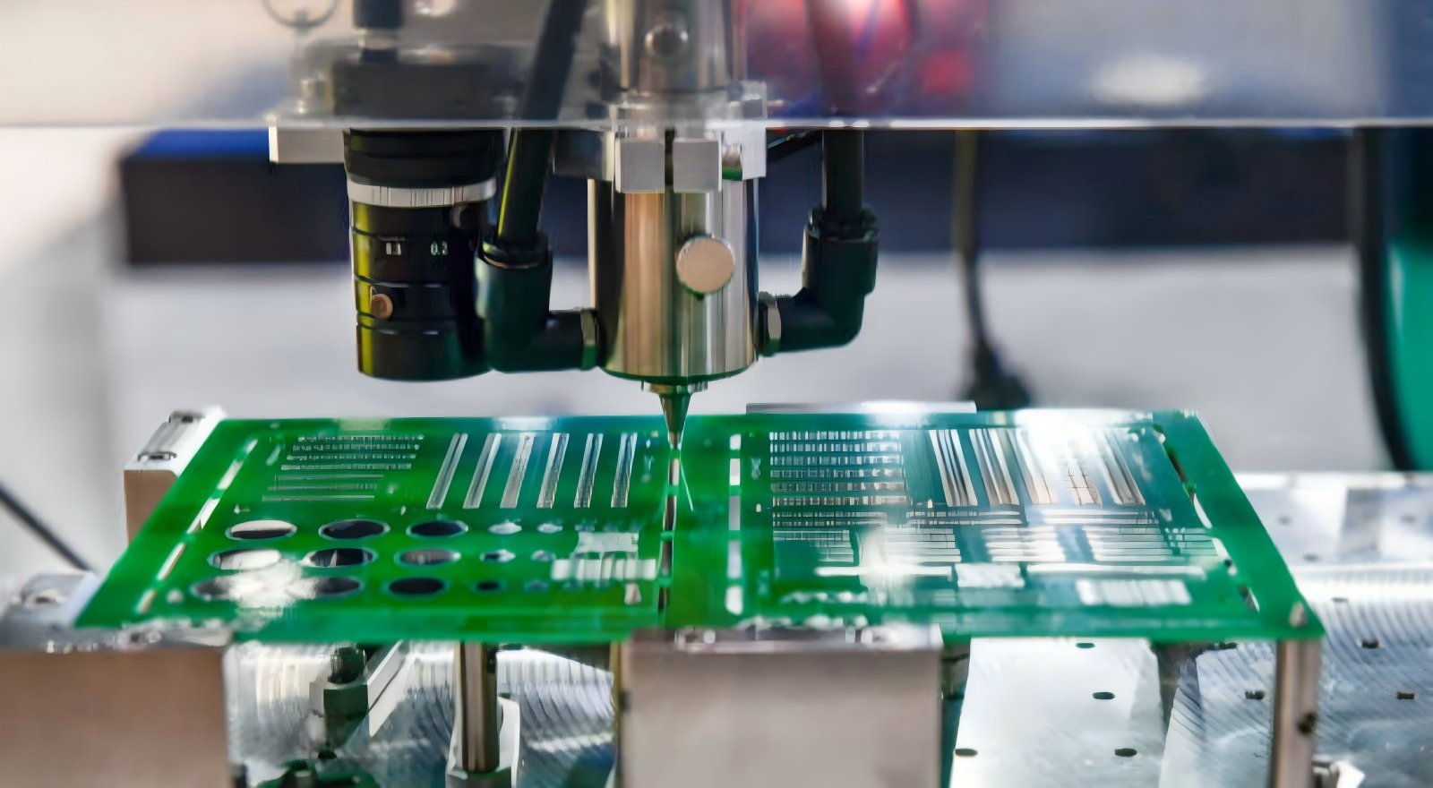
What Is Jet Printing?
Jet printing is a stencil‑less, digital printing method that resembles precise inkjet printing. A printhead deposits micro‑droplets of solder paste onto PCB pads, following CAD design information. The all‑digital process uses no tooling and allows real‑time control of paste volume, dot size and position for each pad.
Key Advantages
Maximum Agility: Change designs in minutes by simply uploading new designs; no stencil waiting time.
Pad‑Level Precision: Enables 0.3‑mm fine pitch and 3D boards, down to a 1 nanoliter per pad dispensing volume.
No Tooling Cost: Saves on stencil cost and time‑to‑market.
Reduced Waste: Only delivers paste needed, consumes 35-45% less material than stencil printing.
Limitations
Longer Production Time: 2-5 minutes per board, not suitable for high‑volume production.
Increased Initial Cost: Fancy equipment is expensive and needs to be used for low‑to‑mid‑volume printing.
Delicate Calibration: Printheads require frequent cleaning and maintenance to prevent clogging and ensure precision.
Stencil Printing vs. Jet Printing
Production Volume
Stencil Printing: Ideal for high‑volume, low‑mix (thousands of the same board). Economies of scale via low cost per unit and speed.
Jet Printing: Best for low‑volume, high‑mix, prototyping and design changes. Tooling cost is zero for small‑batch production.
Design Complexity
Stencil Printing: Ideal for standard, uniform boards with standard pad sizes and pitches. Not suited for large/small pads or 3D.
Jet Printing: Best for high‑density, ultra‑fine‑pitch, multi‑height and rigid‑flex boards. Programs paste volume pad‑to‑pad.
Total Cost Structure
Stencil Printing: High initial cost; low cost per board at high volumes.
Jet Printing: No stencil cost; constant cost per board ($0.50- $1.00) regardless of volume; higher equipment cost.
Turnaround & Flexibility
Stencil Printing: 1-3 days wait for stencil; hours to changeover.
Jet Printing: <10 minute wait for printing; instantaneous design change.
Defect Rate & Reliability
Stencil Printing: Robust, with low defect rates (<50 PPM) with consistent maintenance and processes.
Jet Printing: Ideal for intricate boards, but requires tight control of nozzle positioning and paste properties.
Practical Application Scenarios
Choose Stencil Printing When
Your product is a high‑volume consumer electronics, appliances or automotive module that has a mature design.
Throughput and cost per unit are a priority.
Your boards have standard pitches and pad layouts.
Choose Jet Printing When
You are prototyping aerospace, medical or wearable devices with rapid design iterations.
Your boards have 0.3‑mm fine pitch, mixed component sizes or 3D features.
You require short lead times with no stencil delays or costs.
There is no one "best" method - only the best for your PCB assembly objectives. Stencil printing is the cost‑effective, high‑speed production method. Jet printing is best for flexibility, accuracy, and time‑to‑market for small to medium production. Assess volume, complexity, cost, and time‑to‑market for to improve yield, lower scrap, and improve your competitive position.
For expert advice, cost‑effective assembly services, and expert solutions in solder paste printing and total PCB assembly, contact PCBX - your long‑time partner in high‑quality, cost‑effective, on‑demand production of electronics.
Hot Tags:

Contact us

If you can't find what you're looking for, please contact us.
Article
Choosing between manual and automated PCB assembly depends on production volume, with manual assembly ideal for prototypes and automation best for high-volume runs.
 2026/02/12
PCB stencils ensure precise solder paste application, vital for strong connections and efficient SMT assembly, reducing errors and enhancing product quality.
2024/12/18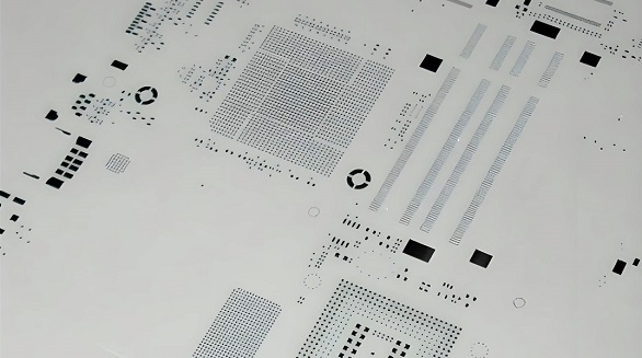
Solder paste stencils are crucial for accurate PCB assembly, offering precision and reduced defects. Various types, including laser-cut and hybrid, enhance manufacturing efficiency and product reliability.
2024/10/22