- Products & Capabilities

- About
- Resources
Wave Soldering Principles and Parameters


Wave soldering, crucial for assembling PCBs with through-hole components, remains vital for producing strong joints efficiently, despite SMT advances, by optimizing key parameters.
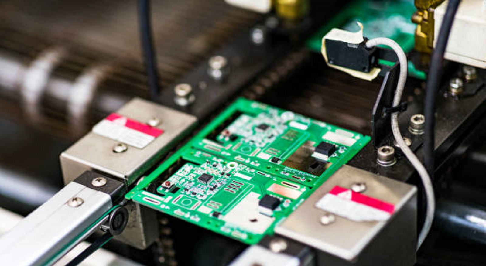
Wave soldering is a basic process of printed circuit board (PCB) assembly, especially in situations where there are through-hole components and mixed-technology boards. SMT has changed the landscape, yet wave soldering continues to be important because it efficiently handles large quantities and forms strong joints. In this article, the fundamentals of wave soldering are discussed, and the essential parameters are examined, along with the problems and solutions related to this technology.
Principles of Wave Soldering
Wave soldering is not a process, but a precise choreography of steps that ensure strong connections between the components and the PCB. The process typically entails four primary stages: fluxing, preheating, soldering, and cooling. All of these stages are the essential components in obtaining high-quality solder joints.
Fluxing: The process begins with fluxing onto the PCB. Flux is a chemical cleaner that dissolves any oxides on component leads and PCB pads to promote enhanced solder adhesion. It also prevents oxidation during soldering. Flux can be applied using various methods such as foam fluxing, spray fluxing, or wave fluxing, and spray fluxing has more control and evenness.
Preheating: Upon the application of flux, the board is preheated. Preheating is necessary to serve the purpose of activating flux and minimizing thermal shock to components as they encounter molten solder. Preheating also guarantees the temperature gradient between disparate elements is upheld, and the possibility of warping or thermal stress is minimized.
Soldering: The essence of wave soldering is the soldering process, during which the PCB passes over one or more dynamic solder waves of molten solder. The solder wave ensures good and consistent contact with the solderable surfaces with sufficient penetration and bonding of the solder to pads and leads. Wave movement is designed to achieve complete solder application without blemish conditions such as bridging.
Cooling: Following soldering, the PCB must be cooled in a controlled manner so that the joints set. Cooling rate must be controlled to prevent residual stresses that can be induced by non-uniform thermal contraction and which would compromise the integrity of the soldered joints.
Critical Parameters in Wave Soldering for Optimum Results
A high-quality solder joint requires careful consideration and optimization of several critical parameters to make them.
Solder Temperature: The temperature of the solder wave is a most critical parameter. It is typically from 245°C to 265°C for the leaded, and 250°C to 270°C for the lead-free. The optimal temperature enables the solder to wet well and flow and bond properly.
Conveyor Speed: This controls the duration of time a PCB spends under the solder wave, usually 2-4 seconds. The conveyor speed needs to be set so that it meets time for soldering without overheating parts and missing them.
Flux Application: The quantity and type of flux, as well as the application method, significantly affect solder quality. Excessive or insufficient flux can form defects such as poor adhesion or leave residues that complicate subsequent processes.
Wave Height: The wave height needs to be adjusted properly to enable the solder to flow to all the necessary areas of the board without causing bridged solder or component displacement. The wave should have complete coverage of the solderable areas and good drainage.
Contact Time: Appropriate contact time between the solder wave and the board is critical to maintaining good heat transfer and the formation of proper solder joints. Insufficient short contact will lead to cold solder joints, while excessive contact will lead to overheating and damage.
Addressing Challenges in Wave Soldering
Wave soldering is a highly effective process, but one with its own set of challenges. It is necessary to recognize those challenges and implement strategic solutions for ensuring solder quality does not suffer.
Component Positioning: Proper alignment is necessary to prevent defects such as bridging or absent solder coverage. Automated placement machines and special fixtures can be utilized to offer accurate positioning and alignment.
Defect Management: The instance of typical wave soldering defects like solder bridging, icicles, and solder balls can be minimized by optimizing the parameters like wave height, conveyor speed, and solder temperature. The manufacturability can also be increased by proper pad sizing and routing design considerations.
Thermal Management: Controlled preheating and cooling cycles make sustained thermal management athermal shock and warping prevention. Application of uniform heat sources and optimized thermal profiles can enhance solder joint reliability.
PCB Design Considerations: Well-designed PCBs that are soldering-aware can efficiently reduce defects. This involves designing for appropriate pad size, maintaining optimal solder mask clearance, and considering component orientation to enable free solder flow.
While SMT is seeing increasingly common application, wave soldering remains a vital method in electronics manufacturing due to its ability to economically produce strong joints in high-volume through-hole and mixed-technology assemblies. By understanding the principles involved and taking careful control of significant parameters, high-quality results can be achieved that meet the rigorous demands of today's electronics market.
Wave soldering is still to be evolved with new processes and equipment, yet it is still relevant and capable of coping with fresh challenges in electronic production. For engineers and manufacturers, the art of wave soldering is still a skill that serves them well, allowing for constant production of high-performing and high-quality electronic products. As technology advances and component miniaturization still occurs, the science and art of wave soldering will still validate its role as a critical manufacturing process.
Hot Tags:

Contact us

If you can't find what you're looking for, please contact us.
Article
Flexible solder masks offer cost-effective flexibility, while coverlays provide durable protection for FPCs, catering to different application needs.
 2025/04/01
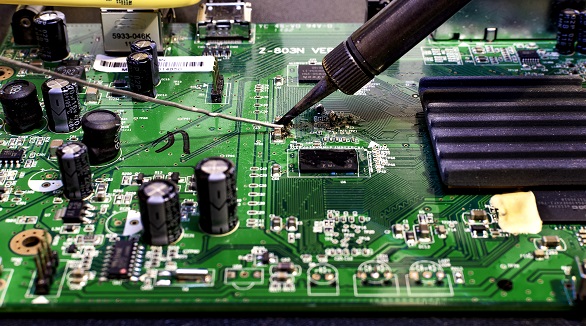
SMD soldering mounts small components on the PCB surface for compact, automated designs but has high setup costs and repair challenges. DIP soldering uses through-hole components for robust, easily repairable, lower-volume applications.
2024/09/24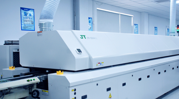
Soldering forms a very important part in the assembly of a PCB. Wave soldering is ideally applied in Through-Hole Technology, while reflow soldering in Surface Mount Technology. Wave soldering involves flux spraying, pre-heating, soldering, and cooling, while in the case of reflow soldering, pre-heating, thermal soak, soldering, and cooling steps are applied. Temperature and time control are the two most critical parameters in the above-mentioned techniques for ensuring soldering reliability.
2024/07/26