
- Products & Capabilities

- About
- Resources
What is High Frequency (HF) PCB?


Learn what high frequency (HF) PCB is, its materials, design rules & industrial applications for RF, radar and wireless electronics.
With the rapid development of wireless communication and navigation systems, along with high-speed data systems, ordinary printed circuit boards using conventional FR-4 substrates can no longer transmit stable signals at frequencies higher than 1 GHz. A High Frequency (HF) PCB is a special type of circuit carrier that is used to transmit radio frequency and microwave circuits only. It solves fundamental issues like high level attenuation, mismatch, EM crosstalk and signal distortion for signals from 1 GHz to hundreds of GHz.
While many engineers are confused about HF PCBs and high-speed PCBs, they are looking for different technical priorities. HF PCBs are designed for best propagation of RF and microwave electromagnetic waves, with stable dielectric loss and consistent wave velocity. High-speed PCBs are used in fast switching electronic circuits, with particular focus on timing matching, signal integrity and clock synchronization. They are similar in advanced communication hardware but have very different material types and rules for layout.
Core Electrical and Physical Characteristics of HF PCB
Because standard FR-4 boards do not have to meet five demanding performance criteria, HF PCBs are not suitable for use in these boards.
Low and constant dielectric constant (Dk): Minimizes signal delay and maintain constant transmission speed in frequency bands.
Ultra-low dissipation factor (Df): Reduces the energy loss within the substrate to eliminate the problems of signal fading in long-distance transmission.
Matched coefficient of thermal expansion (CTE): Resists layer separation during repeated temperature changes, which is matched with copper foil.
Low water absorption: Humidity will affect the Dk and Df; low water absorption ensures that it will perform stable in humid working environment.
Excellent mechanical resistance: High thermal resistance, chemical resistance and peel strength are all there for long term reliable operation in complex environments.
For high frequencies, the dielectric properties of the standard FR-4 materials are not stable and the Df is high resulting in significant signal loss, thus special low loss substrates are required.
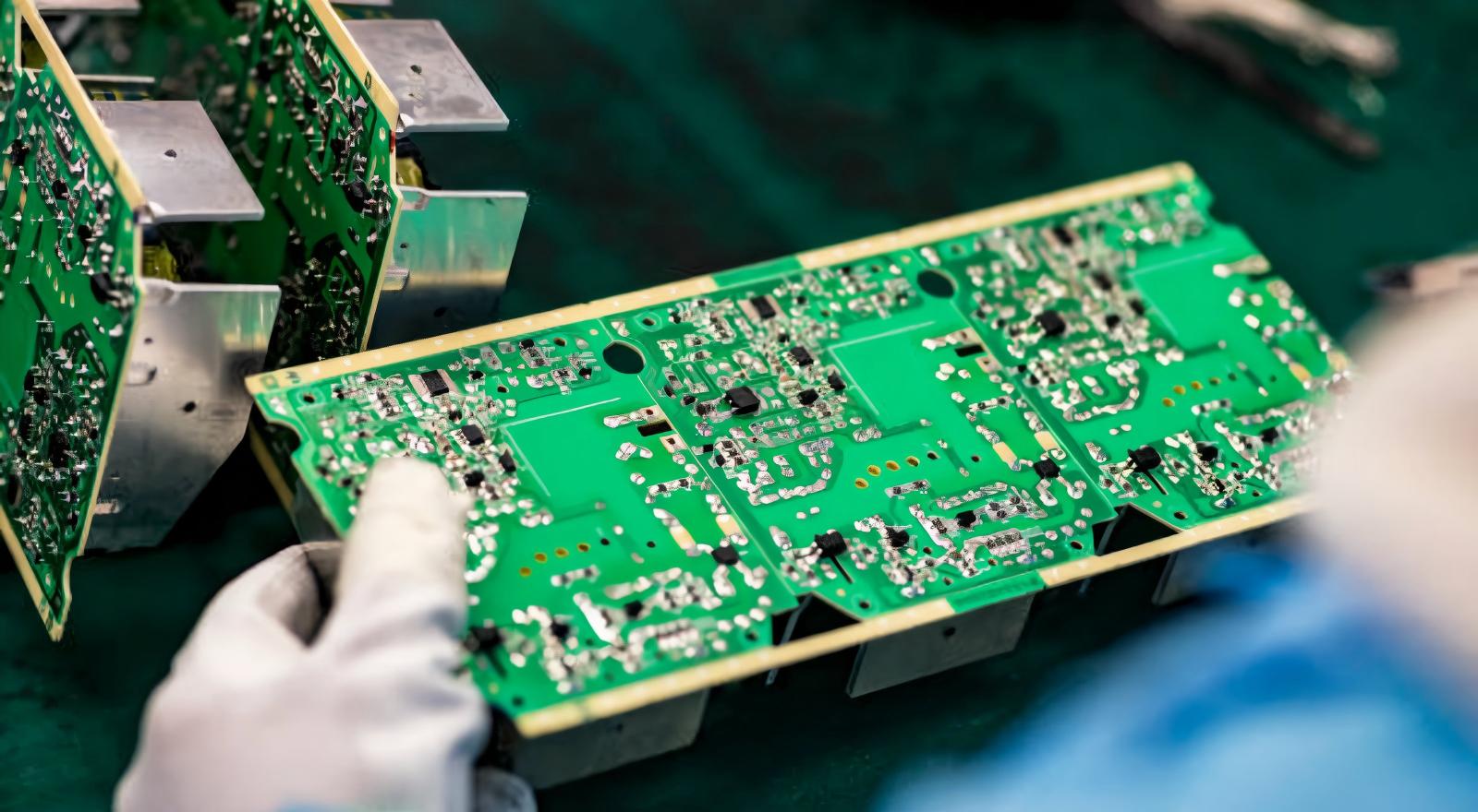
Common Substrate Materials for HF PCB
In the industrial HF PCB industry, there are three major categories of low loss substrate:
Ceramic filled hydrocarbon laminates: Most commercial material. The Dk is stable (3.38-3.48) and low Df (<0.004) at 10 GHz, suiting for 5G RF modules and automotive millimeter-wave radar.
PTFE composite substrates: Have the highest low-loss properties for ultra-high frequency devices like satellite communication and military radar. The major disadvantage is its high material and production cost which restricts its extensive commercial utilization.
Hybrid FR4-high-frequency stacks: Low-to-medium RF situations where a basic high-frequency stack can be coupled with low to moderate fabrication cost.
During lamination and etching, the impedance of all HF substrates has to be kept consistent across the signal traces, which requires micron level precision.
Key Design Rules for High Frequency PCB
The layout of the HF circuits are designed to reject interference and distortion in accordance with unique electromagnetic design requirements:
Trace Routing Optimization
No sharp right angles permitted, 45 degree turns or gentle curves will reduce signal reflection and stray radiation. Designed to reduce the crosstalk—the electromagnetic coupling noise experienced by the parallel wiring segments—designers shorten signal traces. Rarely used due to the parasitic capacitance and impedance discontinuities of each via and the elimination of any via stubs to prevent signal integrity failure.
Noise Suppression Techniques
Sensitive signal pairs are isolated by putting ground traces or full ground planes in between them. The clock lines are orthogonal to the RF traces and not parallel to each other. For layer stack-ups, the 20H rule is used: a power plane is reduced by 20 times the thickness of the dielectrics to reduce edge magnetic flux leakage and RF radiation. A single-point interconnection ensures the separation of analog and digital grounds and prevents harmonic interference. Capacitors are directly coupled to power pins of the IC to remove high frequency noise.
Strict Impedance Matching
Overshoot, ringing and reflection are caused by impedance mismatch. Designers make changes to the width of traces, thickness of copper and the thickness of the substrate to match the load impedance of components with the transmission line impedance to create a continuous signal path. Avoiding large signal loops; if a loop cannot be avoided, then the area of the loop should be minimized.
Main Application Fields of HF PCB
HF PCBs are essential to many high-tech industries:
Wireless communication: RF module for 5G/6G base station, Wi-Fi 7 router and optical transceivers.
Automotive electronics: 77 GHz millimeter-wave radar for smart driving in which it plays a part in obstacle recognition and vehicle wireless collaboration.
Industrial: Enclosures for radar and control equipment, satellite terminals and navigation systems that require reliability in the face of difficult electromagnetic environments.
Precision electronics: High-speed server interconnect boards, wireless testing instruments and medical high-frequency wireless modules.
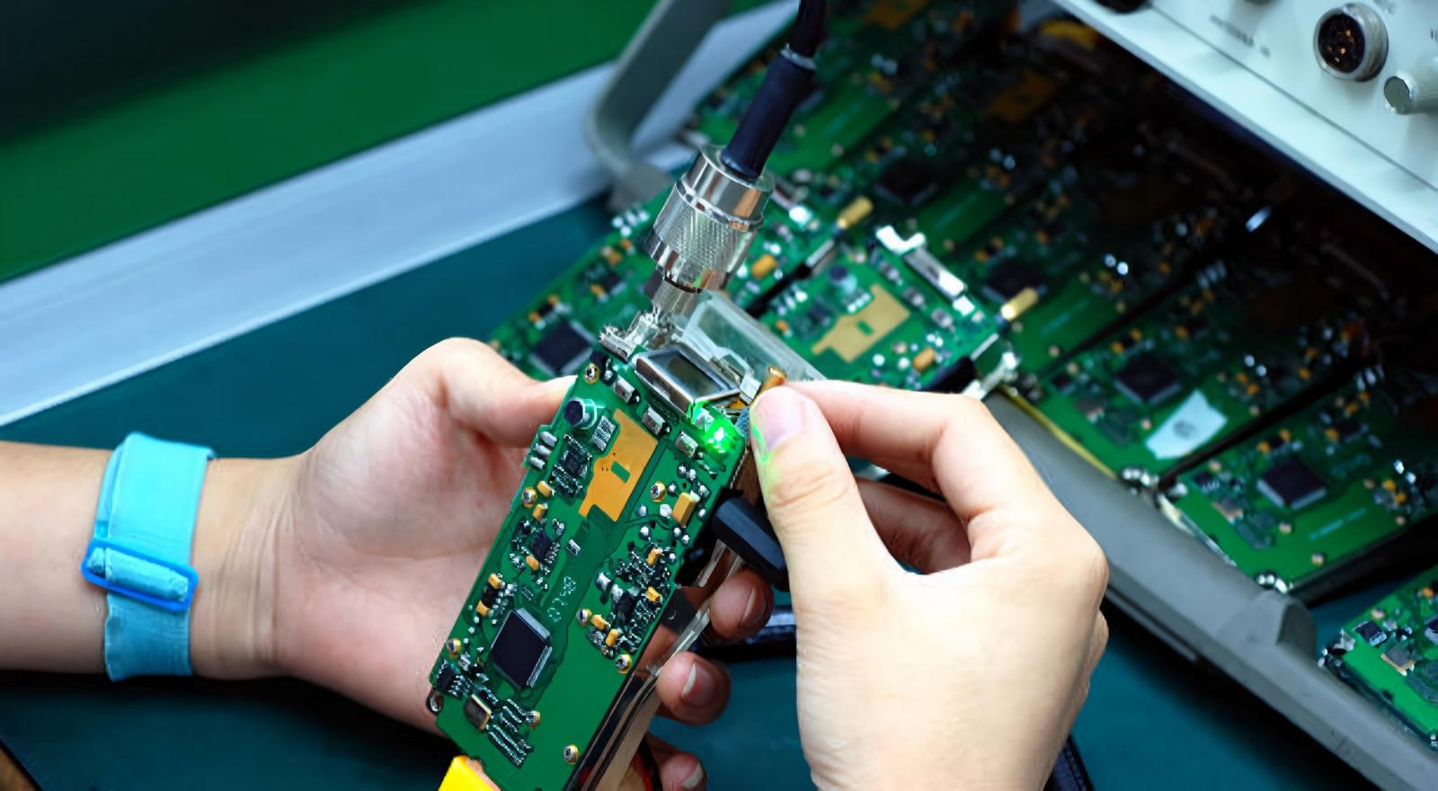
Manufacturing Standards & Production Capabilities
The tolerances in HF PCB fabrication are much tighter than the tolerances of conventional PCBs. Common production requirements are 2 oz minimum trace/spacing, microvias as small as 0.15 mm, controllable copper thickness from 1 oz up to 2 oz and various surface finishes such as immersion gold, OSP and immersion silver to minimize transmission loss. Each completed board goes through automated optical inspection (AOI) and flying probe electrical testing to ensure impedance consistency and circuit connectivity.
As communication and intelligent vehicle technology evolve rapidly, customer demand for high-performance HF PCBs continues to rise. The low loss and high stability of modern RF equipment can no longer be met by ordinary circuit boards. PCBX can offer one-stop high-frequency PCB solutions, including multilayer stack-ups, advanced via process, and full precision manufacturing standards, as well as several complete low loss material options, that address various microwave and RF project requirements by R&D teams and manufacturers who require precise, controlled impedance.
Hot Tags:

Contact us

If you can't find what you're looking for, please contact us.
Article
Any Layer HDI PCBs optimize space and performance with high-density connections, enhancing electronics across industries with reliable, cost-effective solutions.
 2025/04/03
High-frequency circuits face thermal noise challenges. Minimizing resistors and optimizing circuit design can improve performance and reliability.
2024/11/04
High-speed PCBs (>1GHz) are crucial for advanced electronics like 5G and data processors. Key practices include ensuring signal integrity, controlling EMI, and maintaining power integrity for reliable performance.
2024/09/27