PCBX.com Resources
Your source for industry knowledge, news, and expert insights

Latest Posts
Article
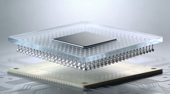
BGAs offer high-density interconnects and compact design, crucial for advanced electronics, but hidden solder joints complicate assembly, requiring precise methodologies.
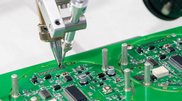
IPC Standards ensure quality, consistency, and global compatibility in PCB assembly, essential for innovation and reliability in electronics manufacturing.
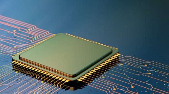
TQFP packages optimize PCB layout with space efficiency, RoHS compliance, and high reliability, addressing die shrinking and enhancing portability.
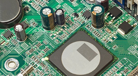
BGA rework stations offer precision, automation, and cost-efficiency, solving challenges in high-density electronics by optimizing component alignment and heating.
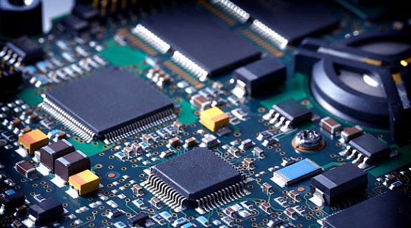
Effective electronic packaging ensures protection, efficiency, and reliability, minimizing risks from environmental hazards and supporting manufacturing processes.
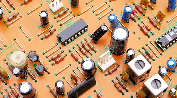
Through-hole assembly remains essential in electronics, offering strength and reliability, especially in critical applications, despite SMT's rise in compact designs.
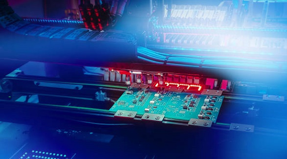
Surface Mount Technology revolutionizes electronics, offering size, cost, and performance benefits, but poses challenges with high setup costs and handling.

Innovative tooling enhances PCBA tab removal by ensuring precision, reducing stress on components, and improving production efficiency and cost-effectiveness.