- Products & Capabilities

- About
- Resources
PCBX.com Resources
Your source for industry knowledge, news, and expert insights

Latest Posts
Article

Learn how to apply DFA guidelines across PCB workflows from schematic to assembly, boost yield and cut production costs effectively.
 2026/05/26
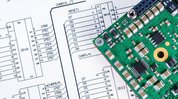
Learn common PCB design mistakes that cause assembly errors and follow DFM best practices to improve PCBA yield and reliability.
2026/05/14
Learn professional copper pour techniques to boost PCB signal integrity, reduce EMI, improve thermal management, and ensure reliable manufacturing.
2026/04/16
Practical anti-ESD strategies for PCB design, including layer stack-up, layout, routing, component use and testing.
2026/04/02
In PCB manufacturing, DFM Checks ensure efficient production by identifying design issues early, reducing costs, enhancing quality, and preventing delays.
2025/05/20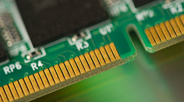
Edge connector bevelling enhances PCB durability and reliable connections, vital for frequent usage and secure engagements, with limitations primarily in plating.
2024/12/25
FR4 permittivity affects PCB signal speed and impedance. It's crucial for design, requiring careful management in high-frequency applications for reliability.
2024/12/16
Schematic diagrams use standardized symbols to illustrate electronic circuits, essential for design, analysis, and construction, bridging concepts and reality.
2024/11/13