- Products & Capabilities

- About
- Resources
PCBX.com Resources
Your source for industry knowledge, news, and expert insights

Latest Posts
Article
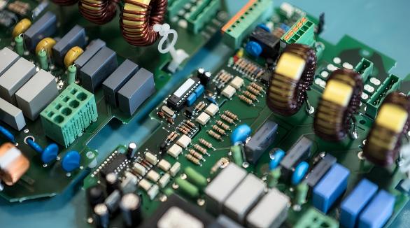
Learn proven PCB layout, grounding & stackup strategies to mitigate EMI, pass global EMC standards for high-speed electronics.
 2026/06/23
Learn what PCB inner layers are, their types, functions, design rules, and common mistakes for reliable multilayer PCB design.
2026/06/09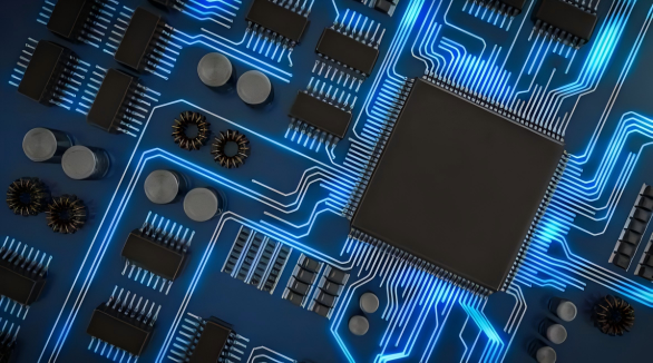
Learn what Chip-on-Board (COB) is in PCB design, covering types, manufacturing process, benefits and industrial applications for compact electronic circuit design.
2026/06/04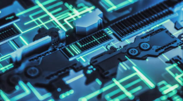
Learn how to apply DFA guidelines across PCB workflows from schematic to assembly, boost yield and cut production costs effectively.
2026/05/26
Learn PCB copper weight standards & balanced copper distribution rules to avoid warpage and boost board stability for electronic design.
2026/05/19
Learn common PCB design mistakes that cause assembly errors and follow DFM best practices to improve PCBA yield and reliability.
2026/05/14
PCB trace repair guide with tools, methods, and tips to fix damaged circuit boards reliably.
2026/04/21
Learn professional copper pour techniques to boost PCB signal integrity, reduce EMI, improve thermal management, and ensure reliable manufacturing.
2026/04/16