- Products & Capabilities

- About
- Resources
PCBX.com Resources
Your source for industry knowledge, news, and expert insights

Latest Posts
Article
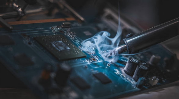
PCB trace repair guide with tools, methods, and tips to fix damaged circuit boards reliably.
 2026/04/21
Learn core component lead forming techniques for axial & radial components, best practices, tools, and defect solutions to boost leaded assembly quality and production efficiency.
2026/04/14
Embedded electronics design focuses on small, low-power specialized computing systems, covering their classification, workflow, applications, benefits, challenges and future trends in modern tech.
2026/03/12
Choosing the right dielectric material for aluminum PCBs ensures effective thermal management, insulation, and reliability in high-power applications like LED lighting and vehicles.
2026/01/08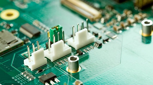
Wave soldering fixtures are crucial for achieving precise through-hole PCB assembly, minimizing defects, and enhancing overall manufacturing efficiency.
2025/12/30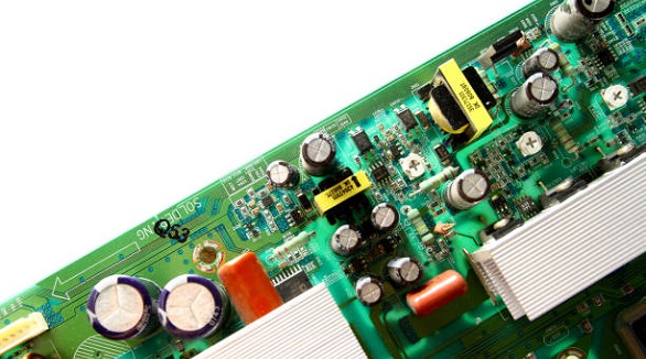
PCB failures due to minor orientation and polarity errors can impact reliability, but proper design practices and checks ensure manufacturability and performance.
2025/12/18
PCB footprints are essential for ensuring accurate component placement, electrical connections, and overall reliability, significantly impacting the manufacturability and performance of electronic devices.
2025/10/11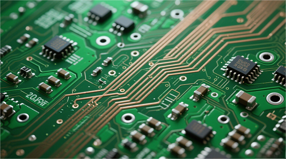
Signal reflection in PCBs, due to impedance mismatches, can be managed with impedance matching, termination methods, and strategic layout to ensure reliability.
2025/09/09