- Products & Capabilities

- About
- Resources
PCBX.com Resources
Your source for industry knowledge, news, and expert insights

Latest Posts
Article
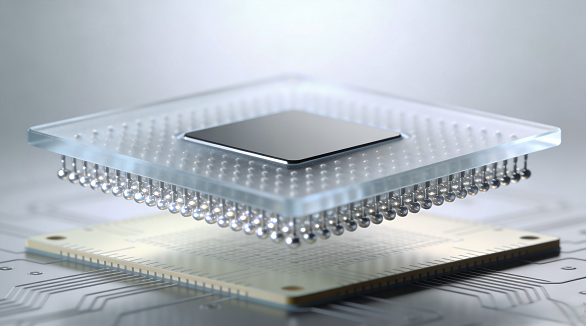
BGAs offer high-density interconnects and compact design, crucial for advanced electronics, but hidden solder joints complicate assembly, requiring precise methodologies.
 2025/12/25
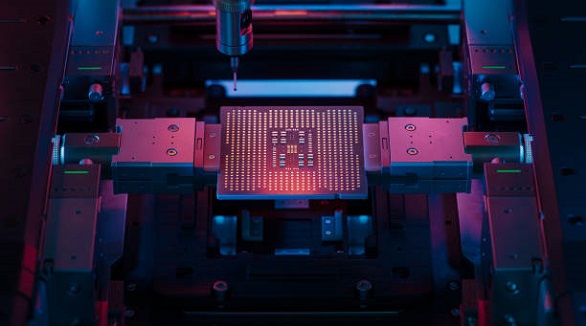
BGAs are vital for compact, high-functionality devices, but demand meticulous routing to overcome design challenges in reliability, manufacturability, and signal integrity.
2025/09/11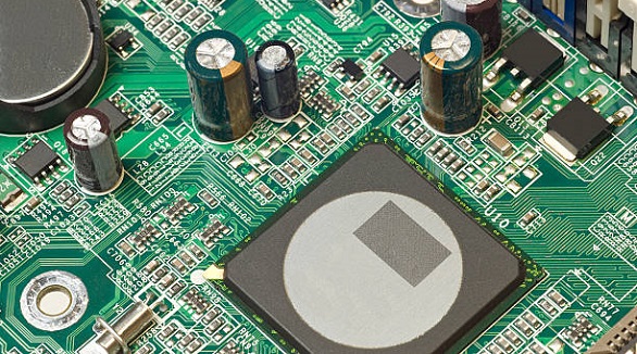
BGA rework stations offer precision, automation, and cost-efficiency, solving challenges in high-density electronics by optimizing component alignment and heating.
2024/12/19
Smartwatches enhance life with health, connectivity, and safety features, supported by tech advances and ecosystem integration, driving market growth.
2024/11/20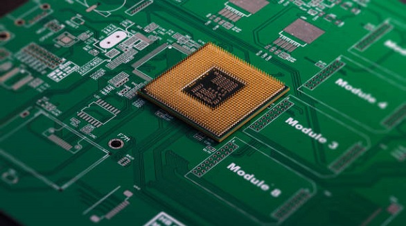
PCB pads connect components on circuit boards. Understanding through-hole, surface-mount, and BGA pads is key for effective PCB design and manufacturing.
2024/11/08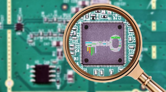
PCB test coupons simulate board elements for reliability checks, detecting early issues to ensure quality and performance before mass production.
2024/10/31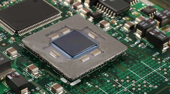
COB technology mounts chips directly on PCBs without packaging, reducing size and weight while improving performance and thermal management, ideal for compact devices like wearables and LEDs.
2024/10/23
Designing PCBs for IoT demands innovation to tackle space, power, connectivity, and security challenges, ensuring robust, efficient, cost-effective devices that meet modern technological demands.
2024/10/18