- Products & Capabilities

- About
- Resources
BGA Routing Guidelines


BGAs are vital for compact, high-functionality devices, but demand meticulous routing to overcome design challenges in reliability, manufacturability, and signal integrity.
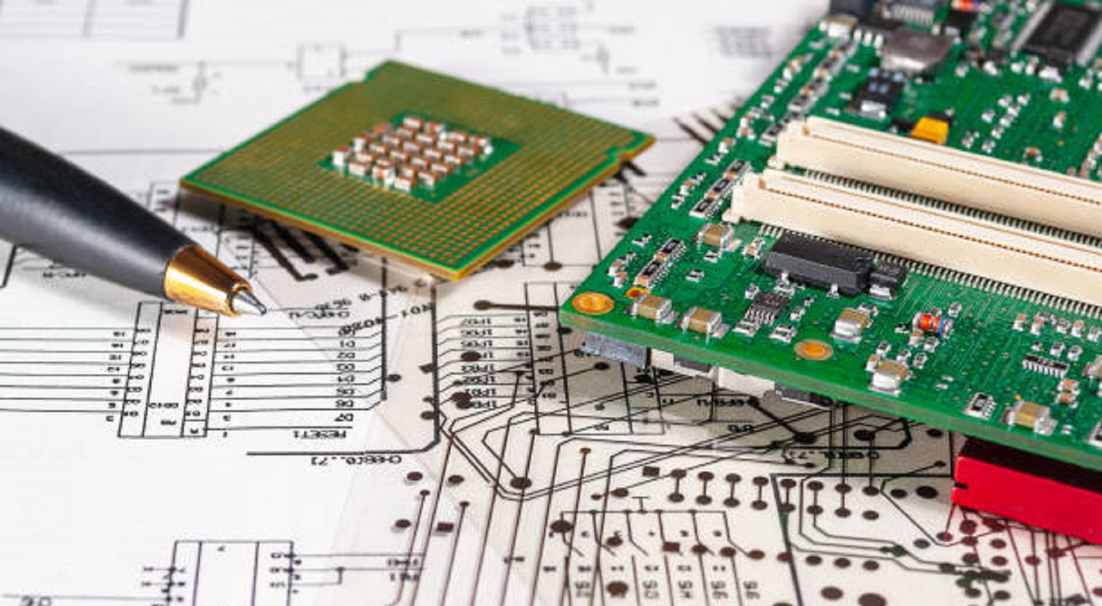
While the pace of electronics advancements picks up momentum, the demand for smaller, faster devices remains committed to pushing the boundaries of PCB design. At the forefront of this technological drive are Ball Grid Arrays (BGAs), the top pick packaging technology for high-end multifunctional devices such as microprocessors and FPGAs. BGAs offer high input/output availability with a small, rugged solution for integrated circuit mounting, but they also present extremely critical design challenges that must be addressed cleverly.
Understanding BGA Packages
BGAs can be further divided into standard and micro types to address specific requirements in PCB design. Micro BGAs are for applications with the smallest amount of space, while standard BGAs are applied in a little more commodious setting. In either scenario, BGAs enable device functionality without adding physical space, and so they are valuable in today's electronics.
Key Challenges in BGA Routing
Although useful, BGA routing poses a myriad of problems that the designer must overcome:
Reliability: PCB reliability is a function of board build quality and where design limits match the capabilities of the manufacturer. Avoidance of good Design for Manufacturability (DFM) practices can lead to non-functional boards or field failures. Some of the issues that require careful consideration to prevent reliability problems are solder mask thickness, copper grain structure, coverlay thickness, and copper weight.
Manufacturability: Preservation of the board manufacturability involves strict compliance with guidelines based on BGA connection routing, via size, pitch spacing, and available layers—driven by manufacturer capabilities.
Signal Integrity: Impedance control is critical to ensure signal integrity, which affects reflection and transmission. They are achieved by trace width matching, the ideal dielectric thickness, and the placement of reference planes between signal layers. Ground or reference planes are also placed between nearby signal traces for crosstalk reduction.
BGA Routing Guidelines
For effective utilization of BGA routing, utilize the following best practices:
BGA Escape Routing Techniques
Dogbone Routing: A minimal solution for isolating the via from the pad by a small trace joining them together, resembling a dog bone. It simplifies manufacturing and eliminates capping and filling of the via, thus eliminating complexity and time.
Via-in-Pad: This is best applicable for minimizing space usage but requires precision to avoid signal integrity issues, like breakout, in which the via extends outside the pad.
Select your PCB stackup depending on the number of I/Os and pinout requirements of the BGA. Define your layers to ensure controlled impedance, having trace widths and dielectric thicknesses matched. Place power and ground planes side by side using thin dielectrics for better power integrity.
Considering Via Options:
Through-Hole Vias: They provide excellent signal integrity and are simpler to implement but take up considerable space.
Blind Vias: Enable more tightly packed designs, staggered or stacked, but introduce additional complexity.
Design Strategies:
Begin your PCB design with the BGA as the center, and ensure that it communicates well with the other board elements. This creates neat routing channels and optimizes layer usage.
Exit paths from the BGA need to deal with signals of varying speeds without introducing crosstalk and noise, and provide good and efficient transmission channels.
Utilizing Simulation and DFM Practices:
Use simulation tools to predict possible power and signal integrity problems. These tools can emphasize parasitic effects and aid in optimizing the board's design prior to manufacture. Including DFM checks guarantees the design will be in concert with manufacturing capabilities, minimizing the chances of costly redesigns.
Overcoming Design Challenges
Implementing these guidelines allows designers to fix common issues associated with BGA routing, conserving time in the manufacturing process and enhancing board quality. Below are some ways you can excel in overcoming some design challenges:
Optimize Initial Layout: Start with the BGA and you can design your PCB layout efficiently. As BGAs are likely to be biggest, they have the capability of driving the floorplanning and setting layer counts and routing scheme.
Define Efficient Exit Routes: Route your BGA's exit routes to efficiently handle high-speed signals with proper spacing to minimize crosstalk and noise.
Power and Ground Planning: Use power rails on one or two plane layers to manage connections more efficiently. Having nearby power and ground planes offers high inter-plane capacitance, supporting power integrity.
The method you use for BGA routing can have significant impact on manufacturability and performance of your PCB design. By following these rules, you ensure the integrity, manufacturability, and reliability of your boards. At PCBX, we are committed to helping designers navigate these intricacies and delivering solutions in alignment with current PCB manufacturing trends and capabilities. Proper BGA routing techniques will enable faster production runs and improved boards to address the stringent demands of advanced electronic devices today.
By adhering to these guidelines and strategies, PCB designers can anticipate issues, minimize manufacturing complexity, and deliver devices which are exceptional in terms of performance and reliability. As the technology continues to evolve, staying abreast of the new trends in PCB and BGA design is crucial for long-term success in the market.
Hot Tags:

Contact us

If you can't find what you're looking for, please contact us.
Article
BGA reballing restores functionality to failed solder joints using precise tools and methods, crucial for compact devices facing thermal, physical, or environmental stress.
 2025/04/29
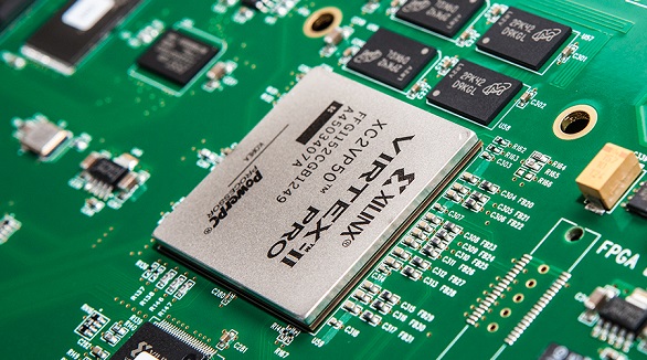
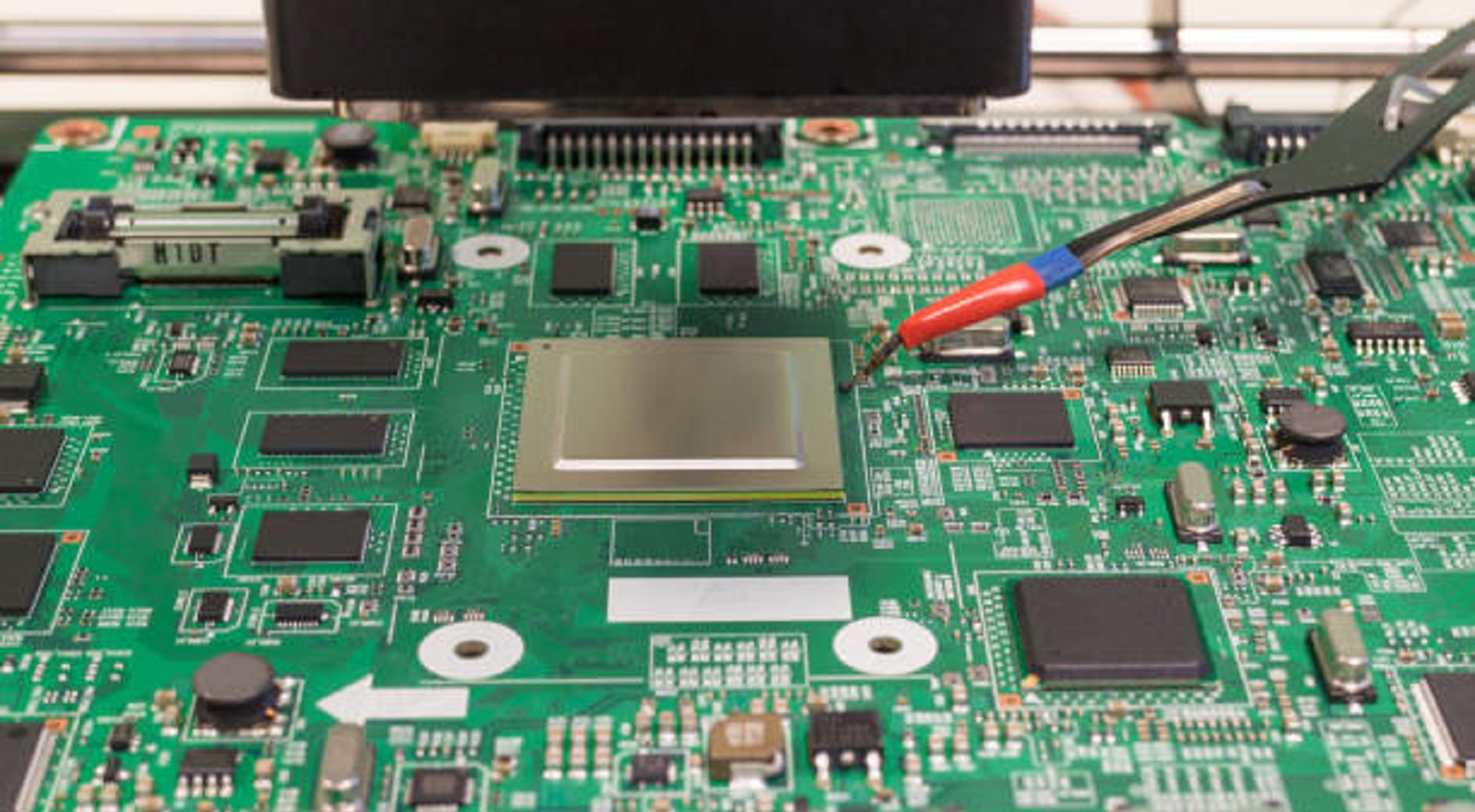
Ball Grid Array (BGA) components, such as PBGA, CBGA, CCGA, TBGA, and CSP, provide high I/O density, improved reliability, and high-quality electrical and thermal performance. Quality assembly and functionality are assured since advanced soldering and inspection methods are required, like AXI and AOI. Proper storage and handling shall guarantee the performance of the devices.
2024/07/26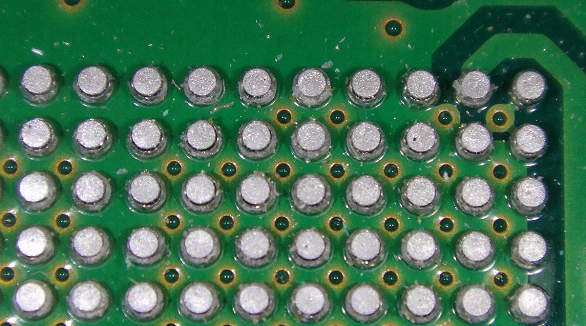
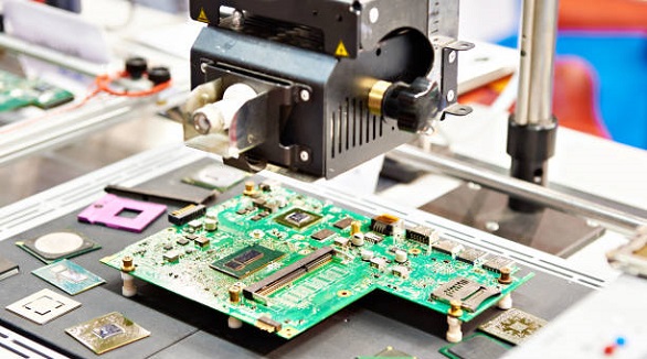
In the late 1980s, when electronics began to shrink, BGA packaging was developed to integrate more connections within a given area. Today, BGA is widely used with high-connection chips—processors being a good example. BGA uses solder balls at the bottom of the chip to connect it to the circuit board. It provides high density along with good heat dissipation and fast signal transmission, one of the main reasons it is ideal for modern electronics. However, it requires precise techniques of soldering in BGA manufacturing.
2024/07/24