- Products & Capabilities

- About
- Resources
Copper Wrap Plating in PCB Manufacturing


Copper wrap plating enhances PCB reliability and performance by strengthening connections, reducing thermal stress, and meeting industry standards like IPC 6012E.
In today's ever-changing world of electronics, reliability has emerged as an essential factor for consumer satisfaction as well as efficiency. Whether it is an LCD monitor working perfectly after five years or it is aerospace technology, it has to be reliable, meaning it has to withstand the test of time. At PCBX, we realize how important it is to integrate cutting-edge manufacturing processes, such as copper wrap plating, into printed circuit boards to ensure longer life and efficiency.
The Imperative of Robust Plating in PCBs
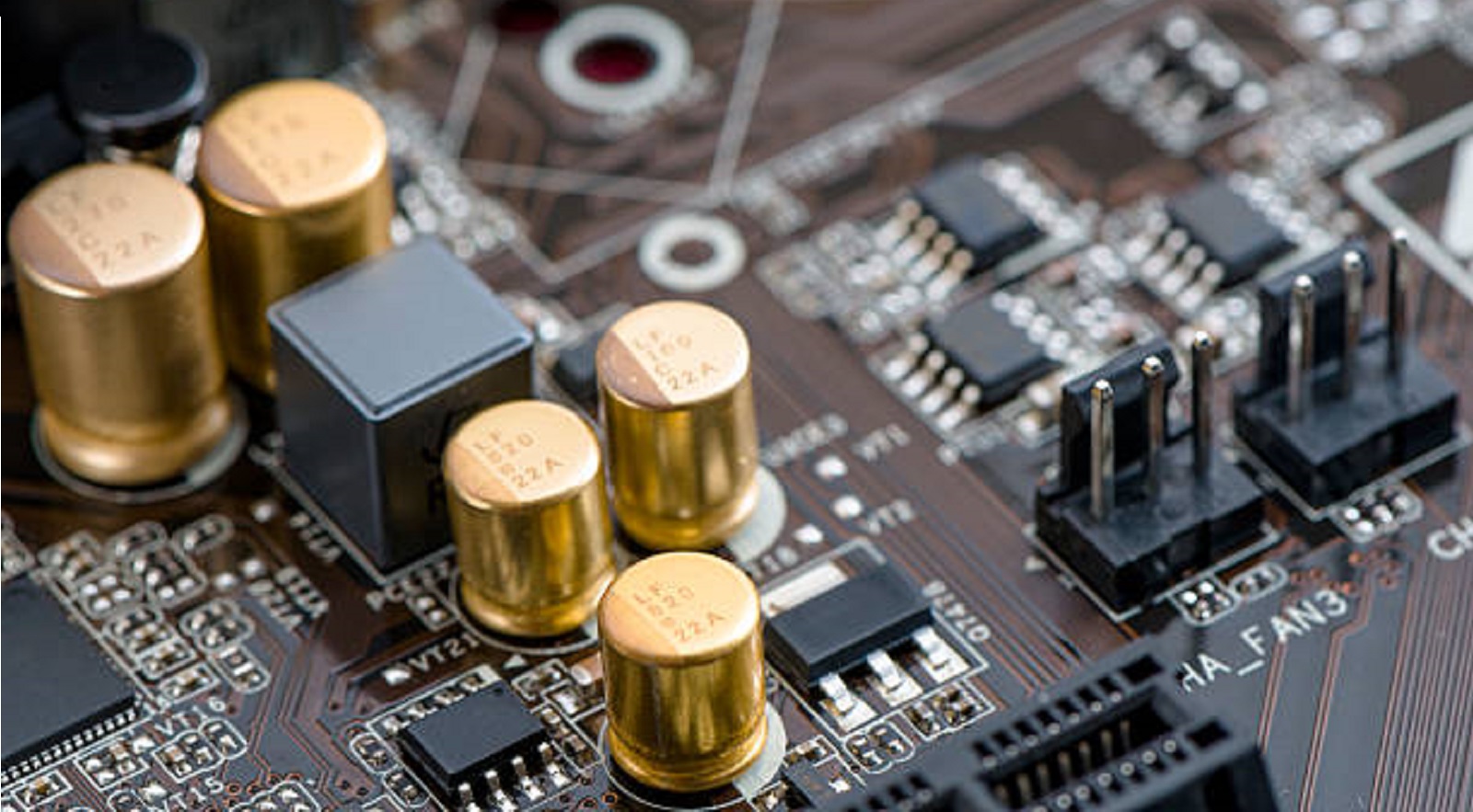
PCBs are basically the hub of all electronic products performing the role of nerve pathways, transmitting signals between each other so as to make the component function. One of the critical elements in the manufacture of these pathways is the plating process employed so as to improve the component’s endurance against mechanical and thermal stresses. Copper Wrap Plating is a new technology that adheres to the standards of IPC 6012E and focuses on improving the reliability of vias-in-pad solutions.
Copper Wrap Plating Process
Copper wrap plating helps to enhance the overall strength of PCBs. This process ensures that there is no gap in the electrical connection between the via hole and the overlay traces. This technique of copper plating helps to cover the outer edge of the via as well as the annular ring surrounding the via pad in addition to encasing the edge of the via.
In copper wrap plating, two major structural techniques are:
Through-Pad and Trace Formation: By coating the inside wall of the through-hole and coppering over the top and bottom layers at the ends of the vias, this configuration forms a good electrical connection through layers in a PCB. An electrical connection is important for signal integrity in layers, as it relates to multi-layer PCBs.
Butt Joint Construction: In this type both pads develop a distinct layer around the ends of the through-hole, which will connect to traces or grounds. While it’s still a non-fully connected joint, the copper layer does add strength to the interface to withstand temperatures.
Addressing Thermal Cycling Challenges
Thermal cycling is an inevitability in PCBs, which occurs during power cycles. The expansion and contraction of the PCB will subject the copper plating to tensile stress. When the PCTs of the materials used in a PCB do not match exactly, added stress caused by the difference is accumulated, resulting in potential breaks. The copper wrap plating process eliminates this issue by adding copper layers.
Further enhancing the robustness of the circuit board, it is also possible to apply cap plating on the wrap plating and add layers on the through-hole top and bottom. Apart from this, this method of circuit board manufacturing is adaptable enough and can be used even on buried vias, making it flexible and adaptable. Additionally, it is able to adhere to the IPC-A-600 standards.
Integrating Multilayer PCBs and Copper Wrap Plating
PCBs with multiple layers have become a need with the ever-increasing push towards mini yet power-packed electronics. These PCBs are able to cater to strict requirements of size and lightness that are necessary requirements of contemporary electronics products. Copper wrap plating is an important part of helping such PCBs become robust and encourage smooth electrical and thermatic flux between layers with their use of effective through-hole connections.
Vias—through hole vias, blind vias, and buried vias—play critical roles in interfacing layers on a PCB. All three require and benefit from the reinforcement provided by copper wrap plating. As a means of providing connectivity between layers or between outer and inner layers and their respective coatings, copper wrap plating ensures that vias are adequately sturdy.
Achieving Accuracy in PCB Production
The production of superior quality PCBs dually requires harmonious adaptation between innovative and excellent design planning. At PCBX, we stress the importance of accurate design integration of copper wrap plating for your PCBs. Our advanced technology helps your printed circuit boards be not only functional but also reliable, meeting and exceeding the IPC standards.
Communication and the design specifications required for manufacturing the boards efficiently and effectively cannot be overlooked. The use of Altium Designer is one such method or software that helps in the effective design of the stack-up, plating, and via structure, which is essential for manufacturability as well as according to industry specifications.
Applications and Advantages
The distinct advantages of copper wrap plating increase its popularity in copious ranges of products, including consumer electronics to industries such as aerospace and telecommunication, where the end products are of extreme importance and thus require the best performance of durability and electrical properties.
Consumer Electronics: Devices that are intended for everyday use demand reliability that can resist normal usage stress. The copper wrap plating used in consumer electronics protects them against damage and makes them last long enough to satisfy consumers.
Aerospace and Automotive: These industries require components to possess the ability to survive in tough environments. The copper wrap plating robustness increases the reliability and perfect functionality of PCBs, even when subjected to mechanical stress and extreme temperatures.
Telecommunications: As the complexity of telecommunication networks develops, the need for PCBs that can properly handle signals at high rates becomes an important aspect. Copper Wrap Plating enhances electrical paths, which reduces the loss of signals, thereby improving communication efficiency.
Copper wrap plating is an innovation that is changing the face of PCB assembly by ensuring that PCBs produced are not only reliable and durable but also have improved functionality when it comes to electronic devices.
Choosing PCBX, you can tap into extensive knowledge and innovative technologies solely focused on enhancing the reliability of PCB. We welcome you to discover how copper wrap plating can help enhance your products and offer the same level of quality and durability that the modern market demands. Request a manufacturing and assembly quote today and begin the journey for optimal performance of your PCB.
Hot Tags:

Contact us

If you can't find what you're looking for, please contact us.
Article
Copper weight determines PCB effectiveness in conductivity, thermal management, and mechanical strength, essential for high performance in various applications.
 2025/08/12
Copper balance is key in PCB fabrication, ensuring signal integrity, thermal management, and reliability by managing copper distribution for efficiency.
2025/08/07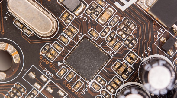
PCB copper plating is key for creating conductive traces that drive electronic circuits, offering benefits like conductivity, anti-corrosion, and cost-effectiveness. Plating methods include electroless and electrolytic.
2024/09/25