
- Products & Capabilities

- About
- Resources
DFA Guidelines: Optimizing PCB Design from Schematic to Final Assembly


Learn how to apply DFA guidelines across PCB workflows from schematic to assembly, boost yield and cut production costs effectively.
The high-performance PCB design is no longer just about electrical correctness and functionality in today's electronic product development. How easy it is to assemble and manufacture a printed circuit board can be crucial to its ultimate success. Design for Assembly (DFA) is a collection of well-known engineering principles that are used to optimize every detail of a design to facilitate automated manufacturing, minimize assembly defects, reduce manual rework, and shorten time-to-market of a product. Many engineering teams experience expensive delays, low first pass rates, and constant design changes just because the principles of DFA are not taken into account until after layout or even after delivery of the file. From schematic capture to the final PCB assembly, integrating DFA throughout the entire workflow is crucial to help bridge the gap between theory and practice. According to industry statistics, if the DFA rules are not followed from the beginning of the design, the total cost of production may be as high as 30%, which makes DFA an essential part of PCB development into the modern world.
Understanding the Unique Value of DFA in PCB Workflows
DFA is very important to differentiate from traditional DFM (Design for Manufacturability). While DFM is more concerned with optimizing bare PCB fabrication processes such as routing, copper thickness and hole design, DFA is more concerned with the whole post-fabrication assembly process, including SMT pick-and-place positioning, reflow soldering, automated optical inspection, and manual rework. The fundamental goal of DFA is to modify the design of the PCB to suit the automated assembly equipment, to replace manual processes and to reduce the most common manufacturing errors such as tombstoning, bridging, under-soldering, and offsetting. From a small batch of prototypes to mass production, it is a great advantage to have a standardized DFA optimization that can help ensure the consistency of the assembly and reliability of the product.
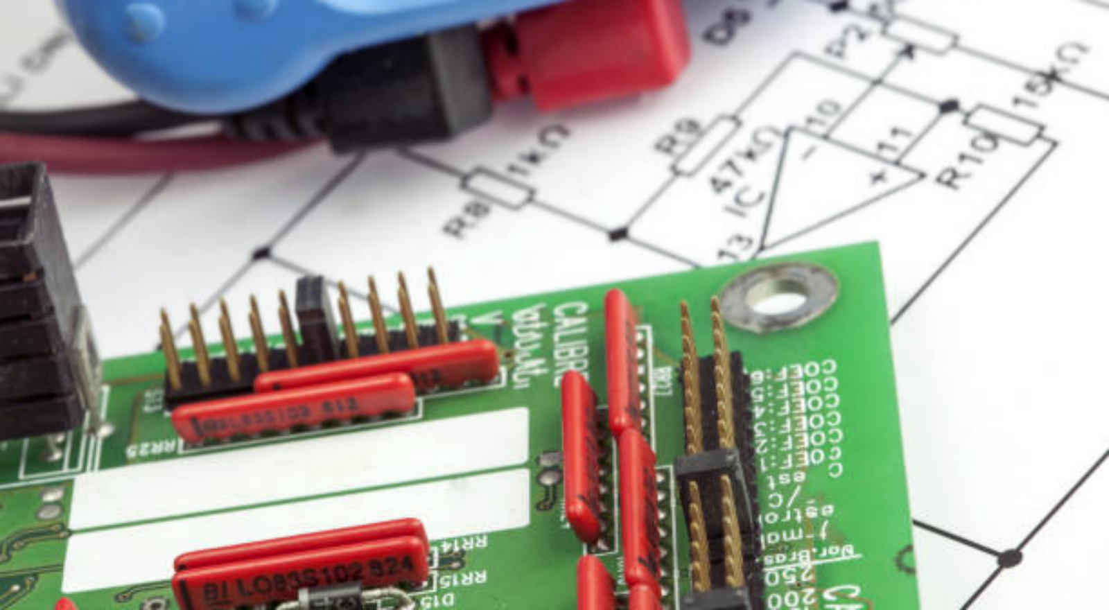
DFA Optimization Starting from Schematic Design
The key to high quality assembly is not to start in the PCB layout stage, but to start with well optimised schematics. Many latent risks of assembly arise because of unreasonable choices of component and non-standard schematic planning. In the schematic design stage, engineers should always choose the common and off-the-shelf components and not the rare, unique or end-of-life components that create a problem in manufacturing because they are not in sufficient supply. At the same time, decreasing the diversity of components and combining the passive components that have similar specifications can help to simplify the factory inventory management and reduce the cost of programming the assembly line.
Another important step in DFA is the creation of a set of standard documents in schematic format. All parts should have consistent part numbers and polarity should be marked on polarised parts such as diodes, LEDs and electrolytic capacitors. Clear and informative schematic labelling helps to avoid placing the part the wrong way round when it is being assembled by an automated machine and helps minimise production inspector judgement errors. Also, during schematic planning, designers must provide test points and positioning fiducials to make sure that layouts are not too tight up later in design.
Key DFA Layout Rules for Assembly Compatibility
The most crucial implementation phase of DFA guidelines is PCB layout, directly affecting the feasibility of assembly and yield. The first is that the spacing of components needs to be carefully adhered to. Small SMT components should be spaced at least 0.5mm apart so as not to cause solder bridging during reflow soldering, and larger power devices should be spaced apart by a sufficient distance for heat dissipation and rework. Avoid placing any components within 5mm of the edge of the board as it may be damaged when depaneling or clamping the fixture.
Unified component orientation is an easy, but powerful DFA practice. When all the polarized and mini types are placed in the same direction, the direction of the pick and place nozzles' motion is consistent, which not only improves the production efficiency, but also simplifies the inspection of AOI. Power regulators, power resistors, and other heat generating components should be separated from heat sensitive components so as not to cause uneven heating and damage to the components during soldering for thermal compatibility. The V-scoring and break away tab design, at a reasonable value, are good for panelized production since they allow for easy breaking without fracturing the neighboring components.
Complete BOM Validation and Final DFA Design Review
BOM validation is an essential DFA process that cannot be neglected. According to statistics, BOM mismatches and wrong part specification make up almost 15% of the PCB delays. To prevent parameter mismatches, engineers must carefully cross check part numbers, packages and layout footprint details. Removing legacy parts, installing alternative part options and indicating special part handling requirements for moisture sensitive parts is also required to maintain a smooth assembly flow.

The last line of defense before production files are released is a thorough DFA checklist review. The following are all part of this inspection: footprint accuracy, solder mask and silkscreen clarity, test point accessibility, thermal layout rationality, and panelization standardization. This approach to the review process identifies any potential problems before they arise, thus mitigating the need for expensive rework and change of design on site. In actual practice, a systematic integration of DFA can lower the assembly cost by 25% and shorten the total production cycles by 15-20%.
DFA is not just a series of “optional” rules, but it is a systematic design thinking approach which permeates the schematic, layout and documentation stages. Considering early integration of DFA helps to avoid inconsistencies between design and manufacture, consolidate assembly quality and increases production scalability. It is important to have professional process support to get standards, high yield and low cost PCB assembly. With one-stop PCB production and assembly solutions, PCBX offers robust and reliable manufacturing solutions that are industry standard and DFA-oriented, as well as helping engineers to create innovative designs into fully qualified products quickly that are ready to market.
Hot Tags:

Contact us

If you can't find what you're looking for, please contact us.
Article

PCB footprints are essential for ensuring accurate component placement, electrical connections, and overall reliability, significantly impacting the manufacturability and performance of electronic devices.
 2025/10/11
Designing a PCB involves ten detailed steps: schematic capture, creating a blank PCB layout, syncing designs, defining stackup, setting design rules, placing components, adding drill holes, routing traces, labeling, and generating output files. These steps ensure an organized, error-free process from concept to manufacturing.
2024/08/29
The article is developed concerning the breakthrough of integrated circuits and the need for custom PCBs in some electronic products. It enumerates ten golden rules in conducting PCB layout design and manufacturing: grid selection, routing, power layers, component placement, panel duplication, component value combination, frequent DRC, flexible silkscreen use, decoupling capacitors, and pre-production parameter checks. These rules provide for the optimum design and manufacturing of a PCB.
2024/07/25