- Products & Capabilities

- About
- Resources
The Significance of a Footprint in PCB Design


PCB footprints are essential for ensuring accurate component placement, electrical connections, and overall reliability, significantly impacting the manufacturability and performance of electronic devices.
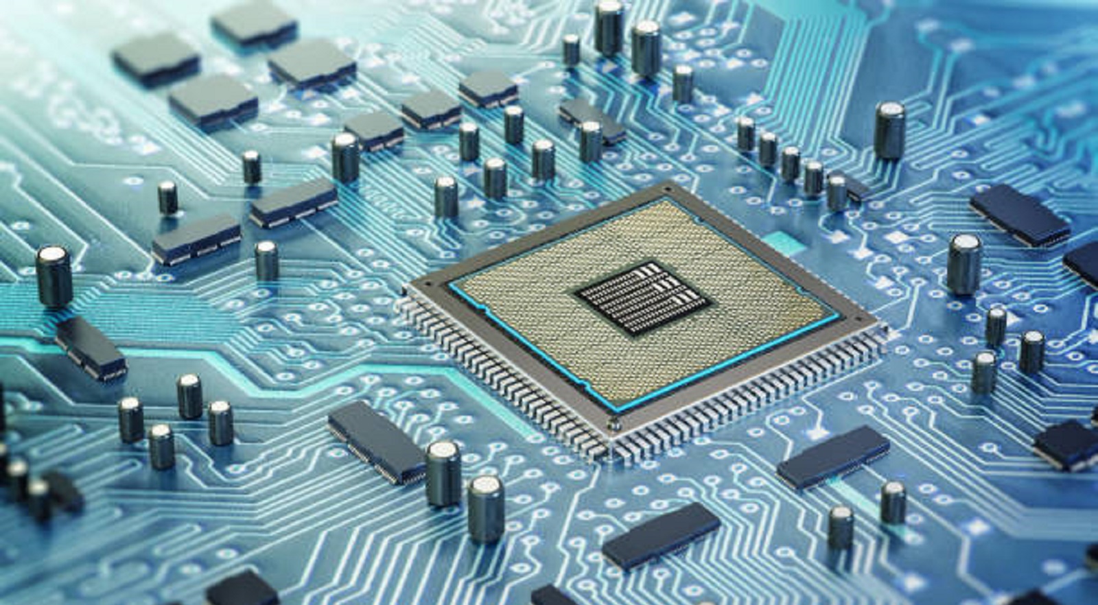
In the fast-changing and modern electronics era, the printed circuit board (PCB) serves as the electrical and structural backbone of almost all electronic devices. Behind successful and error-free PCB function lies a vital design element termed the "footprint." Understanding the significance of PCB footprints and good design practices in designing them can become a difference-maker in making an electronic device successful.
What is a PCB Footprint?
A PCB footprint, also known as a land pattern, is the critical layout on a PCB that corresponds to the physical and electrical specifications of electronic components. Essentially, it is the blueprint that ensures each component is correctly situated on the board with appropriate electrical connections. Whether dealing with surface mount devices (SMDs) or through-hole components, a footprint determines where components are soldered and how they align with other elements on the board.
Critical Aspects of a PCB Footprint
Courtyard and Outline:
The courtyard creates a clean border around the component footprint to avoid interference or congestion due to other components.
Mechanicals:
Mechanicals, such as heat sinks, must be considered since they can influence the spatial positioning without affecting electrical routes.
Hole or Pad Locations:
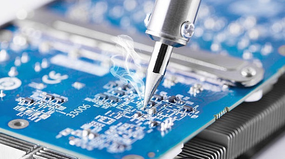
Correct placement of SMD pads and THT holes is crucial for ensuring good soldering and secure electrical connection.
Reference Designator:
An alphanumeric identifier that uniquely identifies each part on schematics and layouts, making the assembly and debugging processes easier.
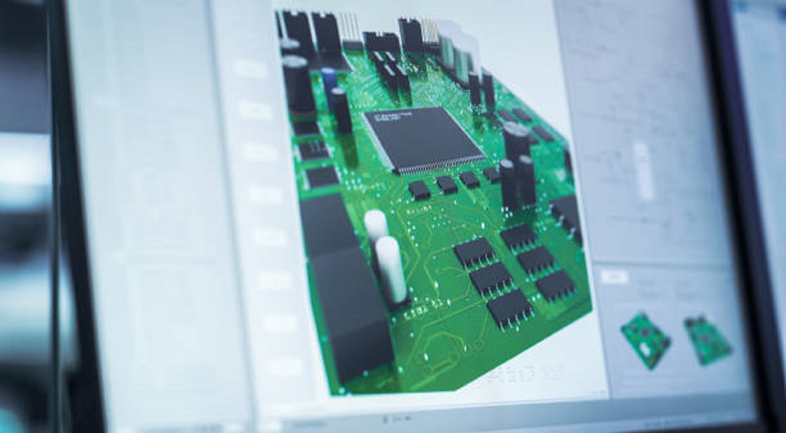
3D Model:
Offers a visual representation for mechanical analysis and allows proper spacing and clearance in a three-dimensional environment.
Pin-1 Designator:
This indicates correct orientation for parts, especially significant for polarized parts like diodes and polarized capacitors.
The Importance of Precise Footprint Design
PCB footprint design is not just an exercise in procedure; it significantly affects the manufacturability, performance, and reliability of electronic products.
Enhancing Electrical Performance
Signal Integrity: Properly designed footprints play a critical role in developing strong and stable electrical connections that are necessary for maintaining signal integrity within the circuit.
Parasitic Reduction: Accurate footprints minimize parasitic capacitance and inductance, critical in optimizing the performance of high-speed circuits and reducing unwanted interference.
Facilitating Manufacturing Efficiency
Automated Assembly Compatibility: Precise footprints are needed for automated pick-and-place machines, reducing the likelihood of assembly faults.
Defect Minimization: Footprints help reduce production defects like poor solder joints or component misalignments by placing components with precision.
Mechanical and Thermal Reliability
Stability Under Stress: Well-designed footprints provide mechanical stability to components, allowing them to withstand stress due to vibration or physical shocks.
Thermal Management: Thermal pads and vias in footprints assist in proper thermal dissipation, which is essential for components that generate a significant amount of heat.
Enabling Cost Effectiveness
Reduction of Prototyping Iterations: Precision footprints reduce the prototyping iterations, saving product development time and resources.
Standardization: Utilizing standardized footprints enables component interchangeability, reducing cost and allowing design reuse across projects.
Enabling Design Flexibility
Easy Modifications: A library of properly designed footprints allows for easy component substitution, making upgrades and modifications a breeze.
Supply Chain Flexibility: Standardized footprints provide flexibility by allowing the use of compatible parts from various manufacturers, which makes the supply chain more robust.
Challenges in Designing Footprints
Designing accurate footprints has its share of challenges that need diligent care and adherence to industry best practices.
Common Challenges
Variation Between Manufacturers: The component sizes vary slightly among manufacturers, and precise and flexible footprint designs are required.
Component Miniaturization: As components become smaller, it requires more accuracy to design footprints for high-density pin packages.
Best Practices in Footprint Design
Start with Accurate Specifications: Utilize complete and accurate component specifications and manufacturer recommendations as a starting point.
Design Systematically: Begin by defining pad sizes and locations, then define the overall component outline and include required mechanical and visual details.
Include All Essential Information: Ensure the footprint contains all the important information, such as pin orientation, polarity markings, and assembly notes.
Check Thoroughly: Carry out rigorous verification to ensure that footprints are correct and complete to prevent costly manufacturing errors.
Meet Industry Standards: SMT designs must follow standards like IPC-7351 or produce consistent, high-quality results.
Standards and Guidelines
Conforming to established industry standards ensures quality and compatibility in various design and manufacturing processes.
IPC-7352: Provides guidelines on creating successful SMT designs and gives the assurance of high-quality solder joints.
ANSI Y32.2-1975: Standardizes schematic symbol sorting by pin numbers, promoting consistent design practices.
ISO 10303-21: Defines 3D STEP model standards, allowing mechanical and electronic CAD system integration.
Avoiding Common Mistakes
Not following best practices results in severe issues, such as:
Small Component Outlines: Create assembly challenges, especially with automated lines, which can increase cost and time.
Incorrect Pad Sizes: Poor solder joints or assembly failure occur.
Inappropriate Pad Spacing: Misalignment during assembly can cause electrical shorts or open circuits.
PCB design footprints are one of the most important determinants of electronic devices' manufacturability, functionality, and reliability. Through adherence to best practices and industry standards, designers can create precise, functional footprints that ensure problem-free production and functionality. At PCBX, we understand the pivotal role played by precise footprint design in the delivery of quality PCB solutions. For expert guidance on how to integrate precise footprints into your designs, contact our team today.
Hot Tags:

Contact us

If you can't find what you're looking for, please contact us.
Article
PTH soldering provides strong connections by threading component leads through PCB holes, requiring meticulous preparation and quality checks for lasting results.
 2025/04/24
Designing PCBs for IoT demands innovation to tackle space, power, connectivity, and security challenges, ensuring robust, efficient, cost-effective devices that meet modern technological demands.
2024/10/18
PCB recycling is vital to reduce environmental hazards and recover valuable materials, especially copper. Effective methods include mechanical, chemical, and thermal processes, significantly benefiting sustainability.
2024/09/27