- Products & Capabilities

- About
- Resources
How to Improve Quality Inspection of PCBs


Rigorous PCB inspections using AI, AOI, and X-ray technology ensure high quality, reduce costs, and enhance efficiency in electronics manufacturing.
In the intricate world of electronics, Printed Circuit Boards (PCBs) are the base that serves as the foundation for an amazing array of electronic devices. At PCBX, we know that very tight quality inspection isn't merely an administrative necessity; it's a strategic necessity that protects the integrity of these essential components and optimizes the productivity of the manufacturing process. Below is a close look at how we can optimize quality inspections and provide the utmost standards for PCBs.
PCB quality testing is essential to identify defects in the early design stage and determine if they meet required specifications. Before large-scale production, it's necessary to check early batches against a number of parameters to confirm that they comply with established quality standards. Proactive steps of this nature help detect defects in the early stage, thereby avoiding reworks and production delays that translate into significant savings and improved operational efficiency.
Types of PCBs and Quality Classifications
PCBs are basically divided into rigid and flexible types. Within the rigid type are further classifications like single-sided, double-sided, and multi-layer boards. Certain inspection processes must ensure that each has to be done by specific techniques meeting different standards of quality categorized as Class 1, Class 2, and Class 3 where Class 3 suggests the highest in requirements. In spite of the differences in technology, general checks of basic quality are applicable across different PCBs for whatever may be the type of PCB as simple or otherwise.
Advanced Inspection Techniques
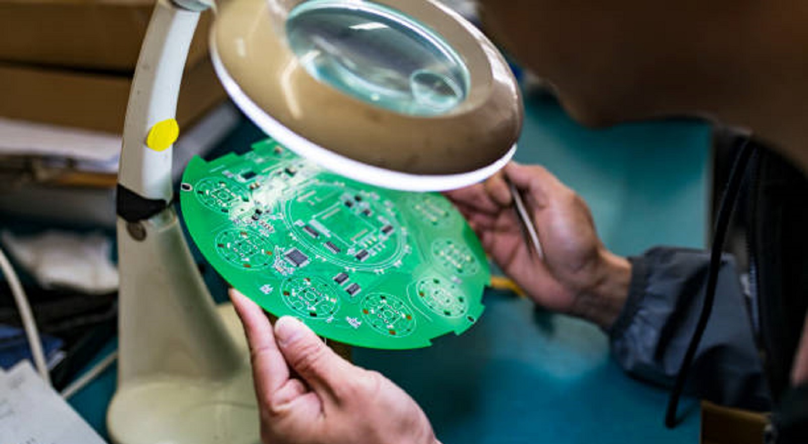
Visual Inspection
Visual inspection remains a cornerstone of the quality assurance process. With basic tools like rulers, calipers, and gauges, inspectors can determine surface roughness, board thickness, and warping. They also examine assembly dimensions and conductive pattern quality for open circuits or short circuits, and measure surface flaws such as pinholes and burrs. Inspectors also examine coating quality, including flux plating, for color and position conformance. Physical Exams
Such physical examinations determine whether any visual or surface imperfections exist, which should be fixed at early stages.
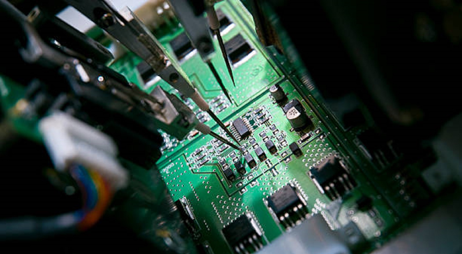
Electrical Inspection
There are two predominant tests of electrical inspection:
Connecting Performance Test: It inspects electrical connectance throughout conducting patterns in ensuring operation within double-sided and multilayered PCBs. Multimeters will mostly be utilized in validating if the connectivity aligns with supporting the desired path for electricity throughout the PCB with no obstruction.
Insulating Performance Test: It is a verification test of insulation resistance, ensuring there is electrical separation between conductors within the same plane or within different planes. The checking precludes any probable short circuit and thereby enhancing overall reliability and safety of the PCB.
General Technological and Metalized Via Inspection
General technology tests address issues related to solderability, verifications for the wetting characteristics of solder onto conductive patterns, as well as the plating materials adhesion. It's essential in ensuring sound, reliable connections in the PCB throughout. Metalizing via inspection is most essential with double-sided and multi-layer PCBs since it examines the metalized vias quality interconnecting layers. It is electrical performance tests by means of open and short circuit methodologies wherein resistance should be between 5-10% and pads are well bonding on metalized vias.
Adopting Better Technologies
Automated Optical Inspection (AOI) and X-ray Inspection
Automated Optical Inspection (AOI) machines utilize high-resolution cameras and sophisticated pattern-matching algorithms to detect defects like component misalignments, soldering defects, and copper trace defects. AOI machines are far faster and more accurate than manual inspections.
For more thorough examination, especially in multi-layer PCBs, X-ray examination is a non-destructive means of evaluating inner structures so that internal defects which are not visible to other examination techniques can be detected. Technology is important for the detection of voids in solder joints and internal short circuits to obtain the highest possible reliability.
Machine Learning and AI Integration
The integration of AI and machine learning technologies can increase inspection capabilities exponentially. AI-based systems offer predictive analysis, detecting trends and probable defects that may elude human inspectors, with accuracy improving over time. These technologies enable a dynamic feedback process, which improves both product quality and manufacturing processes.
Operational Standards and Implementation
Defects are measured by two significant indices: defects per board, measuring the number of defects per board, and defects per million opportunities, a normalization figure over a huge number of boards. These are metrics that allow manufacturers to consider product quality in a comprehensive way and make the necessary decisions to improve and optimize the manufacturing processes.
The use of these high-tech quality inspection techniques puts PCBX at the forefront of PCB production. From design to production and assembly, having complete and technologically sound inspection procedures is crucial. Not only do they enhance product reliability but they also reduce costs of production, with overall efficiency in operation enhanced.
As we go on innovating and improving our processes, PCBX remains committed to achieving unparalleled quality and efficiency in electronics production. By embracing the latest technology, predictive analytics powered by artificial intelligence, and rigorous inspection procedures, we remain dedicated to upholding the highest standards of PCB quality levels, ultimately delivering improved products that serve the stringent requirements of the electronics sector.
Hot Tags:

Contact us

If you can't find what you're looking for, please contact us.