- Products & Capabilities

- About
- Resources
PCB Copper Plating Process


PCB copper plating deposits conductive copper layers on PCBs, forming traces, vias, and through-holes that enable signal transmission, power flow, and reliable multilayer connections.
One of the most important processes in the production of PCBs is copper plating. It develops conductive patterns that enable the transmission of electrical signals and power through the board and relations between different layers in multilayer designs. Modern electronic circuits would not be reliable without copper plating.
What Is PCB Copper Plating?
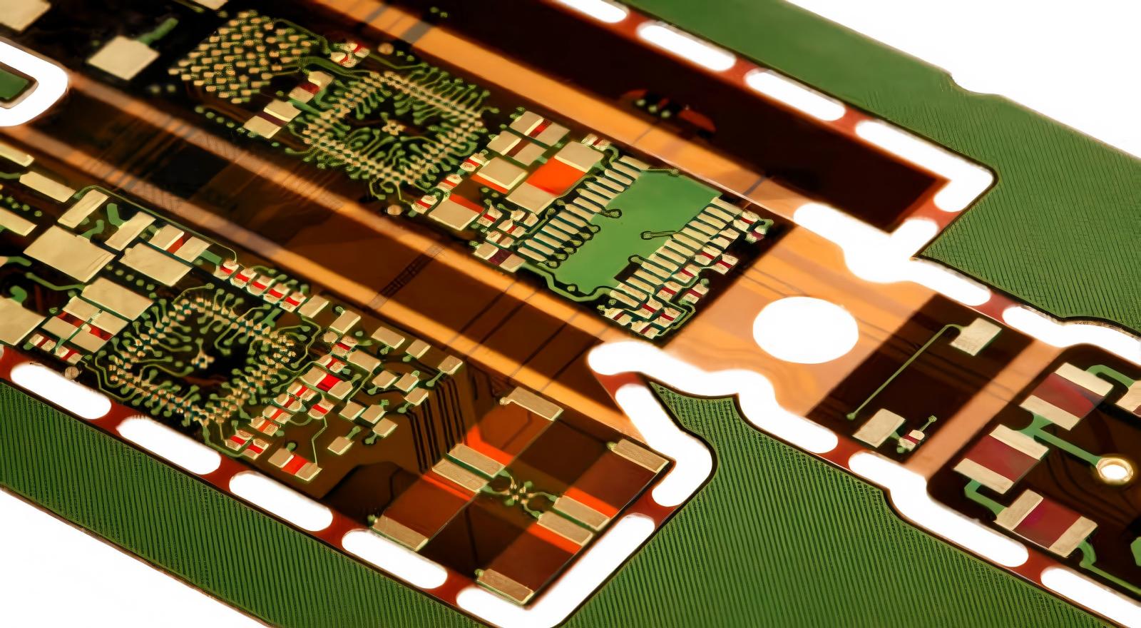
PCB copper plating refers to the procedure of coating a PCB substrate with a copper layer in either a chemical or electrochemical reaction. The plated copper is the traces, pads and vias where the electrical current flows in the circuit board.
Plated through-holes are also created by copper plating the inside of the holes that have been drilled. These are holes that can interconnect several layers in the PCB and conduct signals vertically around the board which is critical in designs of multilayer and high density circuits.
Copper thickness is varying according to the electrical requirements. Thinner copper is commonly used in the inner layers, and thicker copper can be used on the outer layers to carry more current and have better thermal characteristics. Even heavier layers of copper can be employed in power electronics or high-current applications.
Copper in PCB Manufacturing
Copper finds a lot of application in PCB manufacturing due to its superior electrical, thermal and mechanical capabilities.
The high electrical conductivity is one of its greatest strengths. Conducting electrical current through copper has a low resistance hence in electrical circuits; copper is necessary to transmit signals and deliver power efficiently.
Copper is also a good corrosion resister. It is able to create a thin protective layer of oxide which helps prevent further corrosion when left in air. This is a property that enhances the stability of PCB traces in the long run.
Solderability is another valuable advantage. Copper forms a bond with usual solder alloys easily in the assembly process and this enables reliable connectivity between the PCB pads and electronic components.
Copper is also thermally conductive and helps in dissipating heat that is produced by electronic components. Special attention should be paid to effective heat management of high-power devices and circuits with a high density of elements.
Moreover, copper is soft and simple to shape into thin foils that can be overlaid on PCB materials. Copper is much cheaper than other conductive metals like Silver or gold and is therefore the best choice when producing PCB in large quantities.
Major PCB Copper Plating Methods
On PCB fabrication, there are two predominant copper plating processes; electroless copper plating and electrolytic copper plating.
Electroless copper plating is a form of chemical deposition process, which does not require any external electrical power. At this step, the PCB panel is placed in a chemical solution of copper ions and reducing agents. To create a thin copper layer on the substrate and the sides of holes that have been drilled a chemical reaction is used.
It is a very thin layer but it is essential since it forms the first surface of conductivity to further plating.
This is followed by electrolytic copper plating to add on the thickness of copper. During this process, the PCB panel is put into copper electrolyte bath, and a connection with a power source is made. The copper ions in the solution are deposited on the conductive parts of the board by electrical current.
Manufacturers can precisely regulate copper thickness and quality of deposition by modulating plating time, current density and bath composition.
Copper Plating Techniques in PCB Production
The type of plating largely depends on design and production needs of PCB.
In large scale production, panel plating is a common practice. Copper is copper plated on the whole area of the PCB panel and then the circuit pattern is defined. The undesired copper is then removed by etching to produce the desired traces.
Another technique is pattern plating in which copper is plated over only areas of a circuit delimited by a photoresist mask. With this strategy, less copper is wasted and material efficiency is enhanced.
Multilayer PCBs require through-hole plating. Once holes have been drilled, copper is deposited on the walls of the inner holes to join various layers. In Electroless copper, a conductive base is initially produced and electrolytic plating is subsequently used to level the copper layer to provide stable electrical interconnection.
The Main Process in Copper Plating
PCB copper plating process usually starts with the drilling of holes on the PCB panel based on the circuit design. Cleaning and desmearing of drills are done after drilling to remove remnants of drills and resin.
This is followed by chemical preparation of the panel surface by micro etching and activation to enhance copper adhesion.
Electroless copper plating is deposited next as a thin conductive layer over the panel and in holes drilled into the panel. The circuit areas are then patterned with a photoresist layer.
The board is then immersed in electrolytic copper plating bath whereby copper thickness is added to satisfy design requirements. Upon plating, the photoresist is stripped away and the copper that is not used is etched away, generating the final circuit pattern.
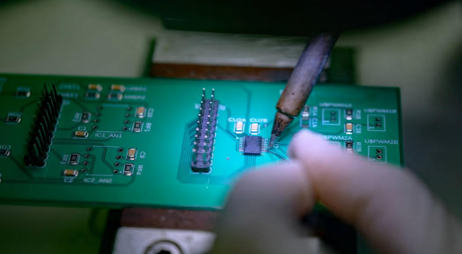
Other operations like solder mask application, surface finishing and electrical testing are then done after the process to complete the PCB fabrication.
Copper Distribution and Plating Quality
Correct distribution of copper on a PCB is significant to the electrical and thermal performance. Lacking uniformity of the copper can lead to heat concentration, signal interference or mechanical stress in the manufacturing process.
Balanced copper designs assist in better heat transfer, decreased electromagnetic interference, and board stability. Designers are trendy towards the use of copper planes and controlled trace spacing to realize optimum circuit performance.
Common Copper Plating Defects
Unless the conditions of plating are well regulated, a number of defects can appear. Pitting may manifest itself as small holes on the copper surface because of contamination or imbalance in the plating bath. The excessive density of current in some sections can result in nodules.
The other problem is the rugged orange peel texture of the surface due to ineffective agitation of the solution. The voids between plates can be formed when some surfaces do not receive copper due to the lack of air bubbles or insufficient flow of the solution.
PCB copper plating is an important process in converting an insulating material into a working electronic circuit. Electroless and electrolytic deposition processes form copper layers which conduct, manage heat and ensure reliable connections between PCB layers.
Hot Tags:

Contact us

If you can't find what you're looking for, please contact us.
Article
Copper wrap plating enhances PCB reliability and performance by strengthening connections, reducing thermal stress, and meeting industry standards like IPC 6012E.
 2025/12/23
Copper weight determines PCB effectiveness in conductivity, thermal management, and mechanical strength, essential for high performance in various applications.
2025/08/12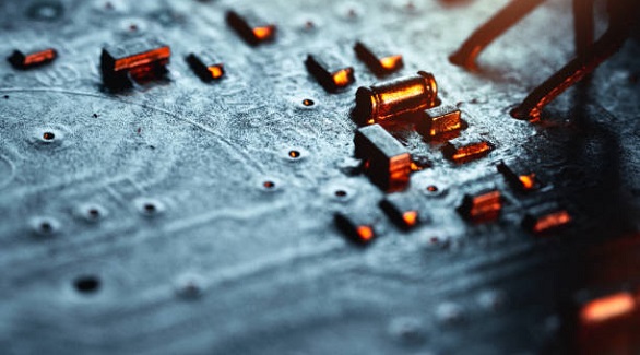
Copper balance is key in PCB fabrication, ensuring signal integrity, thermal management, and reliability by managing copper distribution for efficiency.
2025/08/07