- Products & Capabilities

- About
- Resources
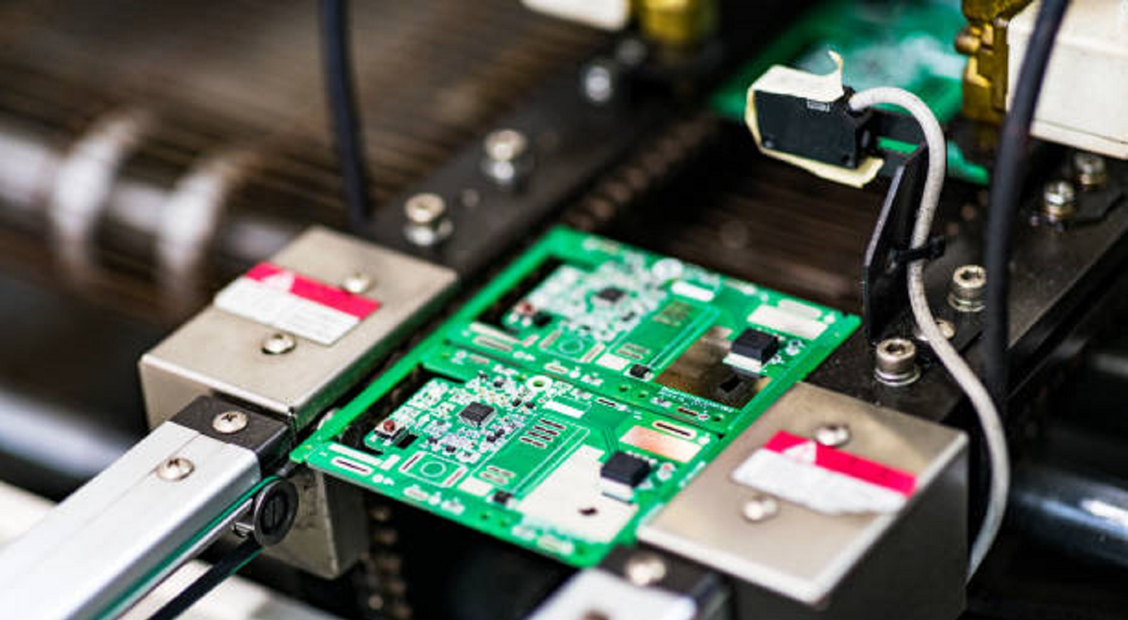
Panel-Plating Blind-Hole Filling in PCB Manufacturing


Panel-plating blind-hole filling enhances PCB reliability and efficiency by integrating filling and plating, meeting the demands of compact, complex, and trustworthy devices.
Innovation is the driving force in the dynamic and rapidly evolving world of PCB manufacturing. Smaller, quicker, and more trustworthy, these are just some of the words that characterize devices in the present time, setting the demanding requirements that PCB manufacturers need to fit into. Another innovative approach that has emerged is panel-plating blind-hole filling-a novel solution designed to economically address the challenges involved in blind vias in multilayer PCBs.
Understanding Blind Holes and Challenges
In multilayer PCBs, blind holes or blind vias are used for important interconnections between different layers. Unlike through-holes, blind vias originate at one surface and end at an inner layer without reaching to the opposite side of the board. This, therefore, makes them quite important in HDI designs where space is a limitation.
Traditional approaches for filling blind holes have a number of drawbacks:
Incomplete Filling: Most of the time, classical techniques leave air pockets or voids, which make the PCB unreliable.
Surfaces: It is relatively difficult to make the entire surface perfectly planar to the board, which may affect the subsequent manufacturing processes.
Tedious Operations: Traditional methods may be laborious; many steps involved just increase the time of production.
Material Waste: Extra filling material should be cleared and is considered waste.
Limited Depth to Diameter Ratios: Traditional methods, such as mechanical drilling, have difficulties with high-aspect-ratio holes.
Panel-Plating Blind-Hole Filling Method
The blind-hole filling method of panel plating directly addresses these challenges through the integration of hole filling with surface plating into one cohesive step. This is an innovative approach wherein a specially designed conductive material is used uniformly to fill up the blind holes, simultaneously plating the board surface.
Key Components and Process
Conductive Filling Material: This is a hybrid material which integrates both properties of plating and filling, hence it effectively performs the integration work and improves electrical conductivity.
Application Equipment: The use of modified plating equipment ensures material application on the entire panel consistently and uniformly.
Curing and Surface Treatment: The special curing process solidifies the filling material; surface planarization is applied afterward for a smooth, even finish.
Step-by-Step Process:
Surface Preparation: Cleaning of the PCB panel is done, which gets it ready for the filling process.
Material Application: The conductive filling material is uniformly applied over the panel surface.
Vacuum Assistance: A vacuum is applied to ensure that the material fully penetrates into the blind holes.
Curing: The panel is then cured in controlled conditions to harden the filling material.
Surface Treatment: Planarization leaves the whole surface with the same thickness.
Final Plating: Additional plating can be done to enhance conductivity and protection.
Advantages of the Panel-Plating Method
Key advantages of this method over classical techniques include:
Filling Quality Improved: The chances of voids and air pockets are greatly reduced, making the PCB more reliable.
Improved Planarity: The process allows the filling material to spread across the entire panel to realize a smooth finish that is useful in further manufacturing processes.
Improved Production Efficiency: Merging filling with plating within one stage cuts production time and minimizes its complexity.
Material Savings: Due to the exact application of filling material, there will be no waste, whereas the traditional methods need excess material removal.
Higher Aspect Ratio Capability: It also enables the filling of blind holes with higher depth-to-diameter ratios, thus allowing more compact and intricate PCB designs.
Improved Reliability: Uniform filling and seamless integration with the surface plating enhance the overall reliability of the PCB.
Applications and Impact on PCB Design
These include the following advanced applications, for which panel-plating blind-hole filling is especially well-suited:
High-Density Interconnect Boards: Best for compact designs featuring several layers.
High-Frequency Applications: The improved quality of fill enhances signal integrity.
Automotive and Aerospace Electronics: Provides improved reliability for harsh operational conditions.
Medical Devices: Miniaturised high-reliability applications.
Further enhancements involve the capability for higher layer counts, support for finer pitch components, enhanced signal routing, and thermal management, thus opening ways for even more complex and efficient PCB designs.
Challenges and Considerations
Despite the benefits listed above, the panel-plating process has some drawbacks that need to be resolved:
Material Development: Success depends upon the conductor filling material. Continuous research has to be done to optimize viscosity, conductivity, thermal stability, and adhesion.
Equipment Modification: Panelplating process needs major modification of equipment presently used for manufacturing PCBs.
Process Control: If material application thickness, curing parameters, and surface planarization must be precisely controlled to ensure consistent results across large panels and over various hole sizes.
Future Developments and Industry Adoption
Future developments within the panelplating method are highly promising:
Material Innovations: Studies on advanced conductive polymers and nanocomposites may point to the way for materials with improved properties.
Automation of Processes: Full automation in the development of panel-plating blind-hole filling could further enhance efficiency and consistency.
Integration with Additive Manufacturing: Finding ways that integrate panel-plating with additive manufacturing techniques for PCBs might yield new fabrication techniques.
Miniaturization: The increase in the limits of hole sizes and aspect ratios that can be reliably filled supports the ongoing miniaturization trends in electronics.
Industry Adoption: Collaboration among manufacturers, material suppliers, and equipment developers will be necessary in the process refinement and creation of standards and guides.
Panel-plating blind-hole filling has been one of the major advances in recent PCB manufacturing technology. Compared with previous art, it integrates the hole filling and plating for greater efficiency, reliability, and design capability in multilayer PCB manufacture. Challenges persist, but the possible benefits from the method make it a very promising direction for future development in the field.
As the electronics industry demands even more compact, complex, and reliable PCBs, innovations such as panel-plating blind-hole filling will be all the more crucial to fulfilling these requirements. Through continued research, collaboration within the industry, and sensitive consideration of technical and environmental factors alike, this technology stands a very good chance of becoming a standard process in manufacturing advanced PCBs to enable next-generation electronic devices. At PCBX, we look forward to continuing our leadership in driving the adoption and refinement of this exciting technology.
Hot Tags:

Contact us

If you can't find what you're looking for, please contact us.
Article
Board and hole plating are essential PCB manufacturing processes, each serving unique roles in ensuring electrical connectivity, mechanical reliability, and overall product quality.
 2025/09/04
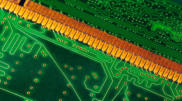
PCB side plating, or edge plating, involves copper along PCB edges, enhancing connectivity, conductivity, shock protection, and assembly, especially for small boards. Used in Wi-Fi and Bluetooth modules, it improves signal quality and EMC. Limitations include necessary design gaps and exclusion of V-cuts.
2024/08/21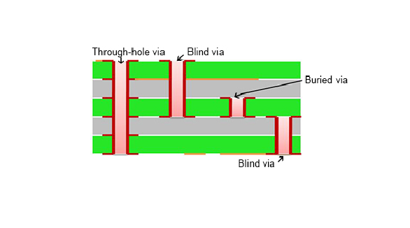
A printed circuit board includes a number of copper foil circuits, which are interlinked by vias. Via (through-hole, blind, buried, stacked, microvias) provides critical interlayer connections in high-density interconnection boards. Blind and buried vias increase the density of boards without adding size; hence, they are imperative for modern trends of miniaturization and high-speed signal transmission. These vias are plated with conductive materials, usually copper, so the electron flow can happen without much effort. Although advanced via types, like stacked vias, cost more, they save up much space and significantly improve routing capacity.
2024/07/26