- Products & Capabilities

- About
- Resources
How to Reduce Ground Bounce in PCB Assembly


Learn practical PCB assembly methods to eliminate ground bounce & SSN, optimize signal integrity for high-speed electronics.
Among all the signal integrity issues of high-speed PCBA production, ground bounce, or simultaneous switching noise (SSN), is one of the most challenging. It's a transient voltage change on ground planes that occurs when a large number of IC input/output pins change logic at once. Ground bounce can cause false logic levels, drift in logic timing, EMI radiation, and sometimes lead to complete system failures – particularly in multi-layer high-frequency boards used in communication, industrial control and consumer electronics applications – where parasitic inductance of ground traces, vias and component leads cause ground bounce. This article combines layout optimization, component assembly specifications, circuit design modifications, manufacturing standards and provides actionable tips for the suppression of ground bounce during PCB manufacturing with a well-balanced technical data and manufacturing guidance.
Root Mechanism of Ground Bounce
The fundamental equation that describes the ground bounce voltage is V = L × di/dt. There is parasitic inductance L present on all conductive paths of PCB. If several outputs switch simultaneously, the transient current flow di/dt produces transient voltages on the ground loop inductance which raises the ground voltage above and below zero volts at the point in question. There are three main reasons behind the severity of the bounces: high loop inductance of the poorly routed power-ground networks; fast slew rates of the devices; and large number of synchronized switching pins. Ground planes are often divided in assembly and long traces for capacitors are used creating even more inductance, and even poorer noise amplitude.
Core Practical Solutions to Mitigate Ground Bounce
Build Low-Impedance Power and Ground Plane Structures
The first and easiest cure for ground bounce is to reduce loop inductance. In order to ensure multi-layer PCBs have continuous, non-segmented solid ground planes to provide the shortest, lowest-impedance return paths for switching current, the ground planes must be continuous and not sectioned with traces. The ground layers should be placed next to the power layers, and the compact dielectric design creates distributed planar capacitance to ensure a quick transient voltage stabilization.
All power and ground is routed short and wide for single or 2-layer boards when no full planes are present, to reduce the trace inductance. Stitch dense vias across ground pours to tie together ground potential and prevent ground islands. Multipin power/ground connections in the package of high-speed ICs provide additional benefit by dividing transient current load and minimize single path inductive noise.
Standardize Decoupling Capacitor Placement and Assembly
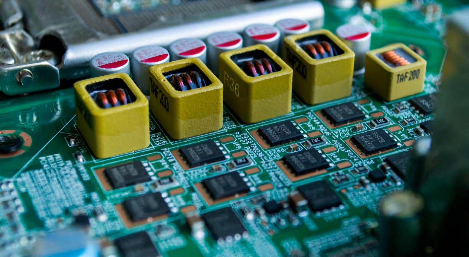
Decoupling capacitors are the most cost-sensitive anti-bounce component, which acts as a local energy reservoir to take up the current surge caused during switching without contaminating the main ground loop. The small high frequency ceramic capacitors 0201/0402 (0.01μF–0.1μF) should be placed within 1mm of the VCC and GND pins of the IC with no long routing traces. Many parallel grounding vias under each Capacitor pad reduces via inductance and enhances high frequency response.
A mixed-value capacitor stack spans over the entire frequency range of noise: small low-value ceramic capacitors are used for handling very fast transients, larger low-ESR MLCCs for voltage droop in the mid-frequency range and bulk electrolytic capacitors for voltage stabilisation in the low-frequency range. If there are layout constraints that do not allow near pin placement, capacitors can be attached to the opposite layer of the board under the targeted ICs to reduce current loop areas. Cold solder joints are eliminated with strict assembly inspection, and will compromise grounding impedance and decoupling performance.
Separate Analog and Digital Ground for Mixed-Signal Boards
Mixed-signal PCBs include noise-prone digital switching circuits with sensitive analog sensors and amplifiers, where ground bounce is able to couple in to weak analog signals, causing measurement distortion. The standardized assembly layout divides the board into separate digital ground (DGND) and analog ground (AGND) areas where all high-speed switching devices and digital ICs are kept in the DGND areas.
The two ground domains are tied together only at a single point at the main power input with a zero-ohm resistor or ferrite bead to prevent high frequency ground bounce from sneeping into analog circuits. Shared high inductance return paths are eliminated and analog module reference voltage remains clean with isolated grounding.
Restrict Simultaneous Switching and Control Signal Slew Rate
The largest ground bounce peaks occur in mass synchronized I/O switching, which means that hardware and firmware changes help to disperse current surges. The rate of rise or fall of the output signal can be slowed by placing 22–100Ω series damping resistors on the IC output pins, which limits the di/dt. Choose ICs that have adjustable drive strength for their outputs and determine the minimum output drive current required for timing purposes. Firmware optimisation delays switching between multiple channel data buses to prevent simultaneous switching of all data bus pins in bulk.
Another aspect of component packaging that affects bounce is the type of package used: BGA and CSP packages have short lead inductance, which reduces the noise sources at the assembly stage.
Optimize Via Layout and Assembly Process Controls
A parasitic inductance is formed by the Vias and a sparse, long Via causes major instability and loss in ground performance. Use arrays of short through-via connections between the grounds of the components or other parts and the ground plane near high-speed switching chips to spread transient current over dozens of parallel conductive paths. Do not use a deep blind or buried via for grounding, as the longer the barrel the more it will increase in inductance.
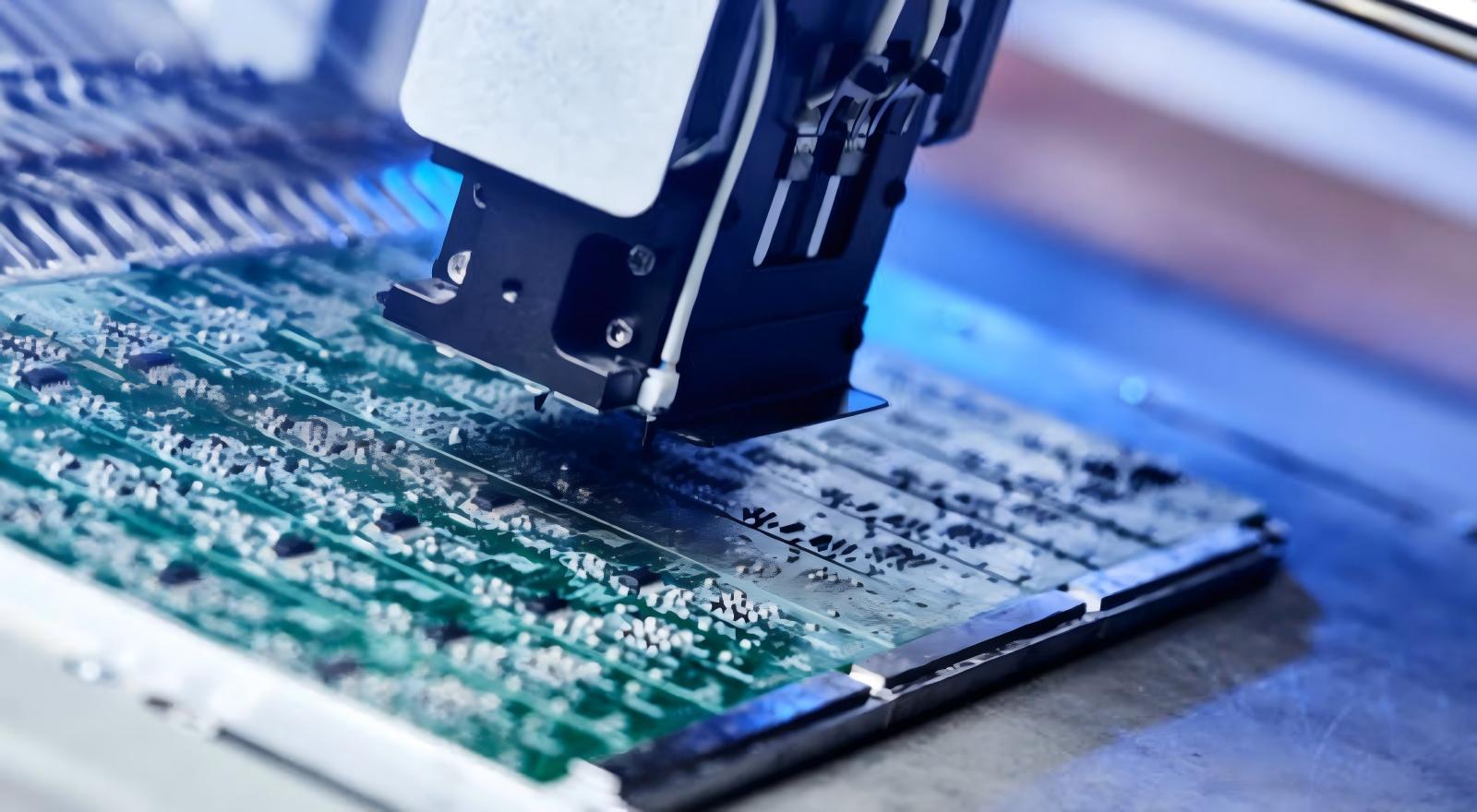
Quality checks after the assembly are a complement: automated optical inspection programs check the full soldering of capacitors and via connectivity, and oscilloscope tests record the ground plane voltage bounces to determine bounce amplitude. Repeated changes of capacitors and capacitor positions reduce noise to acceptable design limits.
The process of ground bounce mitigation requires a multi-layer approach of PCB design and manufacturing of the assembly where the emphasis is to minimize loop inductance, maintain a stable ground reference potential and distribute peak switching currents. Together, continuous ground planes, carefully positioned multi-value decoupling capacitors, isolated analog-digital grounding, slew rate control and dense grounding vias work together to effectively suppress ground bounce noise. The rigorous SMD assembly quality control also ensures signal integrity of high-speed electronic hardware.
If PCB designers and manufacturers are looking for reliable, high performance PCBA services with optimized signal integrity workflows that will allow them to avoid ground bounce, crosstalk and EMI problems for all high frequency board projects, PCBX delivers customized layout consultation, precision component assembly and full signal integrity testing to eliminate ground bounce, crosstalk and EMI issues for all high-frequency board projects.
Hot Tags:

Contact us

If you can't find what you're looking for, please contact us.
Article
Learn common PCB design mistakes that cause assembly errors and follow DFM best practices to improve PCBA yield and reliability.
 2026/05/14
PCB failures due to minor orientation and polarity errors can impact reliability, but proper design practices and checks ensure manufacturability and performance.
2025/12/18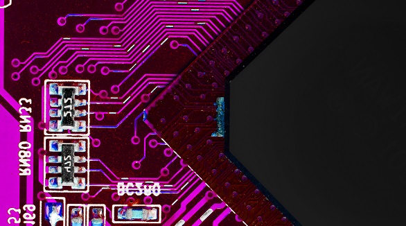
High-speed PCBs (>1GHz) are crucial for advanced electronics like 5G and data processors. Key practices include ensuring signal integrity, controlling EMI, and maintaining power integrity for reliable performance.
2024/09/27