- Products & Capabilities

- About
- Resources
The Ultimate Guide to PCB Trace Repair


PCB trace repair guide with tools, methods, and tips to fix damaged circuit boards reliably.
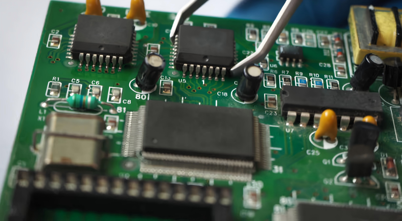
Modern electronics is built upon Printed Circuit Boards (PCBs). Their traces of copper are sometimes only a fraction of a millimeter wide and are used to provide signals and power between components. In case of such traces, any small fault will disrupt performance or result in failure of the entire device.
PCB trace repair thus becomes a critical skill to engineers, technicians as well as highly skilled hobbyists. Through proper methods, one can easily repair broken boards and get them back up on time and with confidence without the need of replacing them.
Understanding PCB Trace Failures
PCB traces can be made of copper, 1 oz/ft2 (35 μm) typical. Their carrying capacity is determined by the width, thickness and temperature increase. As an example, a thin external trace (0.25 mm) is safe with a current of approximately 1 amp at normal conditions, but overcurrents above this may cause overheating and eventual burning.
Trace failures can typically be of two types:
Open circuits: Complete stops that interrupt current
Degraded paths: Partial damage leading to greater resistance
Even minor imperfections may cause an impedance mismatch that causes signal reflection or noise in high-speed circuits.
Typical Trace Damage Causes
The trace damage may be caused due to various mechanical and environmental factors:
Physical Stress: Scratches, bending, or hitting of handling
Overheating: Overheat due to soldering iron, or electrical overload
Corrosion: Exposure to moisture, oxidation or chemicals
Defects or Aging: Low adhesion or material fatigue
Understanding the underlying problem can also be useful in ensuring the repair process is effective, as well as durable.
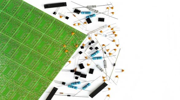
Tools Required for PCB Trace Repair
The key to successful repair lies in accuracy and control. An average installation consists of:
Temperature-regulated soldering iron with a fine tip
Solder and flux to be well wet
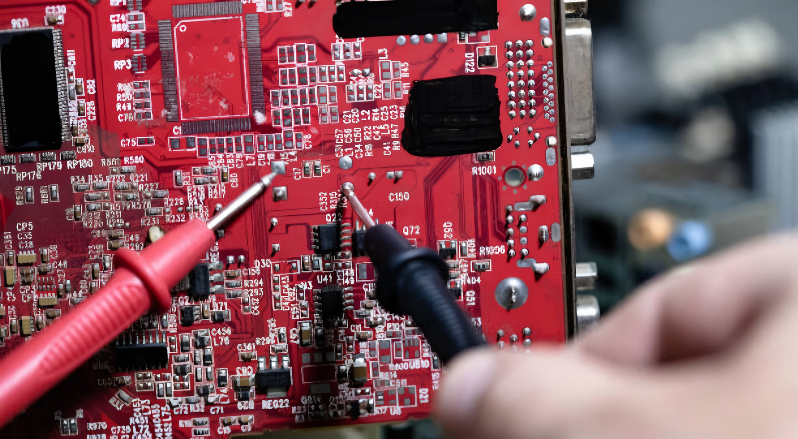
A continuity/resistance checking digital multimeter
Magnification (microscope or loupe)
Surface preparers, precision blades or fiberglass pens
Thin insulated wire (e.g. 30 AWG)
Disinfectants such as isopropyl alcohol
In more complex repairs, conductive ink or copper foil could also come in handy.
Step-by-Step Repair Process
Inspection and Diagnosis
Begin by analyzing visually with magnification. Look for:
Burns or discolouration
Broken or lost copper
Elevated cushions or fissured parts
Check continuity using a multimeter. A good trace must exhibit close to zero resistance at short distances.
Surface Preparation
Clean up the damaged part before repairing. Clean dirt and oxidation as well as protective coating (solder mask) off the break. It is important to expose 2-3 mm of clean copper on both sides to achieve a good connection.
Selecting the Right Repair Technique
The correct repair method will vary according to the amount of damage:
Hairline Cracks (Minor Damage)
Use a small trace of solder and flux to strengthen the trace
Or, conductive ink can be used when operating on low-current
Small Breaks
After exposing the two ends, bridge the gap with solder
Minimise solder to prevent short circuits
Severe Damage (Missing or Burned Trace)
Use a jumper wire to reconnect the circuit
Strip, tin and solder the wire between two fixed points (pads or vias)
Make the wire as short and as straight as possible
Large Area Damage
Foil with copper to re-trace.
Apply solder and fix it to the board.
Reinforcement and Protection
Following the reconnection:
Epoxy or UV-curable solder mask
Make sure that there is insulation against surrounding traces
Secure any jumper wires, mechanically
This will safeguard the repair against vibrations, moisture, and damage in the future
Testing and Validation
The key of success is testing:
Check continuity through the area of repair
Check for shorts with adjacent traces
Start powering the board gradually, preferably by current limiting
In sensitive circuits, ensure signal integrity is maintained.
Advanced Considerations
High-Density PCBs
Present-day boards can contain very small traces (≤0.1 mm between traces). Repairs will need steady hands, lighting and magnification to prevent accidental bridging.
Multilayer Boards
In case internal traces are broken, it is more complicated to repair. In other scenarios, jumper wire rerouting is the only viable option.
High-Frequency Circuits
For RF or high-speed digital designs:
Keep trace geometry constant
Keep away long jumper wires which may serve as antennas
Minimize impedance discontinuities
Best Practices to Avoid Future Damage
Although repair is a good thing, prevention is always better:
Apply regulated soldering temperatures (usually 260-300℃)
Do not subject connectors and boards to repeated mechanical stress
Keep PCBs clean and dry
Design with sufficient spacing and width of current loads
PCB trace repair is an exact but very useful art that integrates electrical concepts with practical application. It is either a small scratch that needs to be addressed properly or it is the major pathway that needs to be rebuilt, but the point is that it should be diagnosed, executed and tested properly.
Since electronic devices are still developing towards an increasingly dense and complicated state, it is all the more useful to be able to fix them instead of throwing them away. PCBX is a reliable partner that can deliver quality and innovative PCB solutions to engineers and companies that need quality and reliability in PCB design, manufacturing and long life.
Hot Tags:

Contact us

If you can't find what you're looking for, please contact us.
Article
Common PCB assembly defects, their root causes, and proven prevention methods are outlined to improve reliability, yield, and manufacturing efficiency.
 2026/02/10
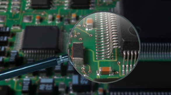
PCB traces, vital for electrical connectivity, can suffer from stress, corrosion, or heat damage, and are repaired by careful inspection, cleaning, and soldering.
2026/01/13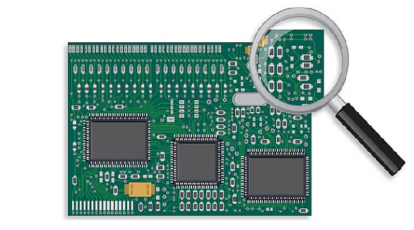
Routine inspections and proper maintenance of capacitors and resistors in PCBs reduce failures, prolong device lifespan, and lower maintenance costs.
2024/11/04