- Products & Capabilities

- About
- Resources
What Is PCB Assembly Line?


PCB assembly lines turn bare PCBs into functional electronics through automated soldering, precise component placement, inspection, and testing processes.
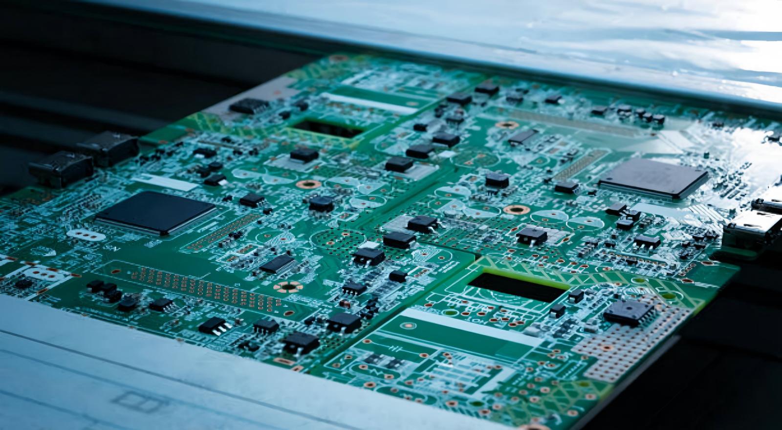
Practically all electronics, whether in modern electronics manufacturing or not, are based on a printed circuit board (PCB). However, a fabricated PCB cannot operate on its own until it is mounted with various electronic parts and through electrical connection. This change occurs in a PCB assembly line, a well-organized manufacturing system where the bare circuit boards are turned into full-fledged electronic assemblies through automated processes and quality control.
PCB Assembly vs. PCB Fabrication
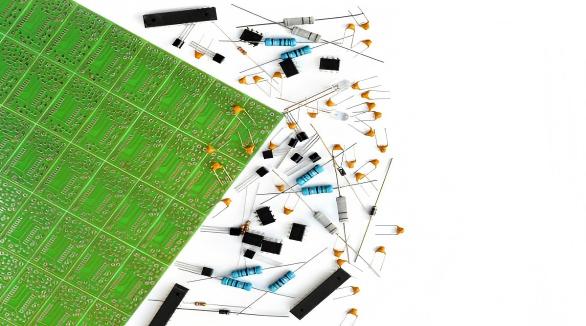
PCB fabrication involves the production of the physical board by etching copper circuits onto an insulator material, whereas PCB assembly (PCBA) involves the placement of electronic components onto the physical board to facilitate electrical functionality. Assembly is the process of attaching electronics components like integrated circuits, resistors, capacitors, connectors and sensors, on specific pads, then soldering them in permanently. Since reliability demands a strong focus on precision and control of the process, assembly can frequently be the most stressful phase in the production of electronics.
What Is a PCB Assembly Line?
A PCB assembly line is a synchronized process of automated equipment and inspection areas linked together by conveyor systems. The stages handle a certain task and retain production flow enabling manufacturers to attain high precision, quality, and output that is scalable. Contemporary lines are highly dependent on automation and data surveillance to reduce human error and ensure a stable performance of manufacturing.
PCB Assembly Process
Pre-Production and DFM Review
A Design for Manufacturability (DFM) review is a pre-assembly analysis by engineers to ensure that the PCB layout is manufacturable. This inspection examines component spacing, pad format, and possible thermal or soldering hazards. Early problem identification will help avoid defects in mass production and waste materials and rework.
Solder Paste Printing
The first mechanical procedure is the solder paste deposition on component pads by a stencil or jet-printing system. The paste is composed of small particles of solder and flux, which provisional connects the components together to be eventually subjected to heating to form electrical connections. The volume and alignment of pastes are also critical as they directly affect the quality of solder joints.
Solder Paste Inspection (SPI)
Automated inspection systems are used after printing to check the height, volume, and position of pastes to maintain consistency. Early identification of printing defects avoids assembly failures further down the production chain and enhances yield of the production.
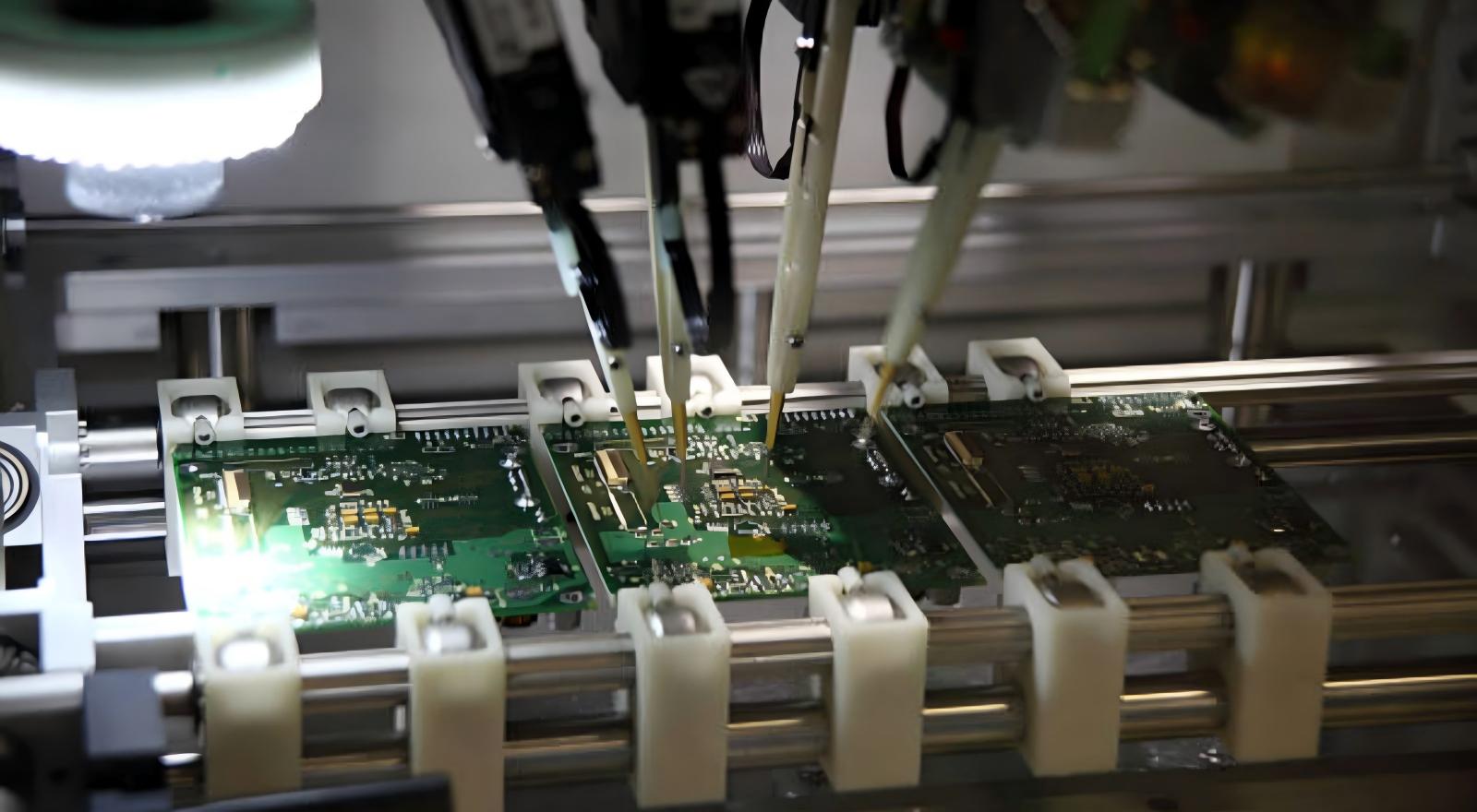
Pick and Place Component Mounting
The ready PCB is then transferred to pick-and-place machines, which place surface-mount components precisely on the solder paste. Vision systems examine the position of the component as robotic heads swiftly load thousands of parts in a single hour. At this level, elements are in place but not fixed.
Reflow Soldering
The board goes through a reflow oven where controlled heating melts the solder paste and creates high-strength metallurgical connections between the components and PCB pads. Properly controlled temperature traces deliver dependable joints without breaking delicate components. In the case of double-sided assemblies, the same can be done on the opposite side.
Through-Hole Assembly (As needed)
Dried holes are made to insert some components which need mechanical strength or more current capacity. These components are soldered through wave or selective soldering and form mixed-technology assemblies, commonly a combination of surface-mount and through-hole components.
Inspection and Quality Control
Automated optical inspection (AOI) systems are used after soldering to check the board against defects, like solder bridges, misalignment, or parts missing. To check concealed joints in the complex packages, X-ray inspection could be employed. They are inspections that guarantee correct assembly before electrical testing.
Functional Testing
Real operating performance is validated with electrical testing, which involves the application of power and signals to ensure appropriate behavior of a circuit. In-circuit and functional tests are employed to verify that every PCB is designed to the specifications and can be used in practice under the stated requirements.
Final Assembly and Packing
During the last phase boards can be swept off, finally inspected and then can be put into packages to be assembled into a complete product. The correct handling safely secures the assemblies against electrostatic discharge and physical damage in transit.
The Importance of PCB Assembly Lines
The combination of automation, precision, and repeatable quality control in PCB assembly lines facilitates modern electronics manufacturing. They enable manufacturers to create complex electronic systems at high efficiency without compromising on consistency of reliability, fewer defects as well as scalable production.
Effective PCB assembly could not only be achieved by using high-quality equipment but also through optimization of design and process stability in the early design. In combination with automated placement, controlled soldering, and inspection, we at PCBX can obtain high yields and reliable product functionality.
A PCB assembly line is a very structured production process that converts a fabricated circuit board into an operating electronic device. The process involves several steps which include design verification, solder paste application, automated component placement, soldering, inspection and testing, all which provide accuracy and reliability demanded by modern electronic products. With technology just becoming dynamic, efficient and smart assembly lines are still critical in providing high quality electronics on large scale.
Hot Tags:

Contact us

If you can't find what you're looking for, please contact us.
Article
Common PCB assembly defects, their root causes, and proven prevention methods are outlined to improve reliability, yield, and manufacturing efficiency.
 2026/02/10
PCBX offers reliable, low-cost, low-volume PCB assembly with custom specs, superior quality control, and excellent customer support, ensuring high customer satisfaction.
2024/08/15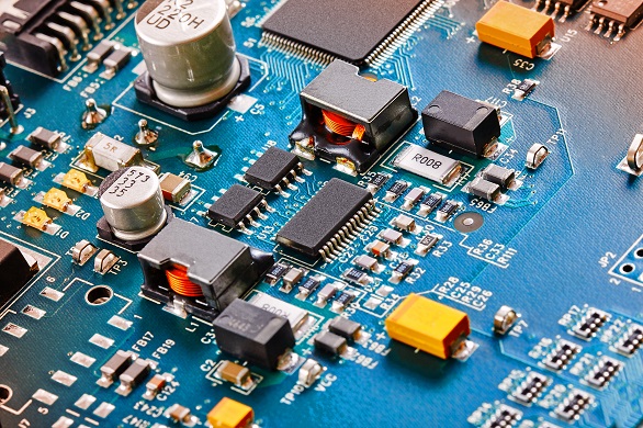
PCBX offers fast, high-quality turn-key PCB prototype assembly services, including fabrication, component sourcing, and testing, all at competitive prices, to accelerate product development.
2024/08/14