- Products & Capabilities

- About
- Resources
What is PCB Routing?


PCB routing is crucial for transforming schematics into functional layouts by ensuring electrical connectivity, signal integrity, and manufacturability amidst evolving design challenges.
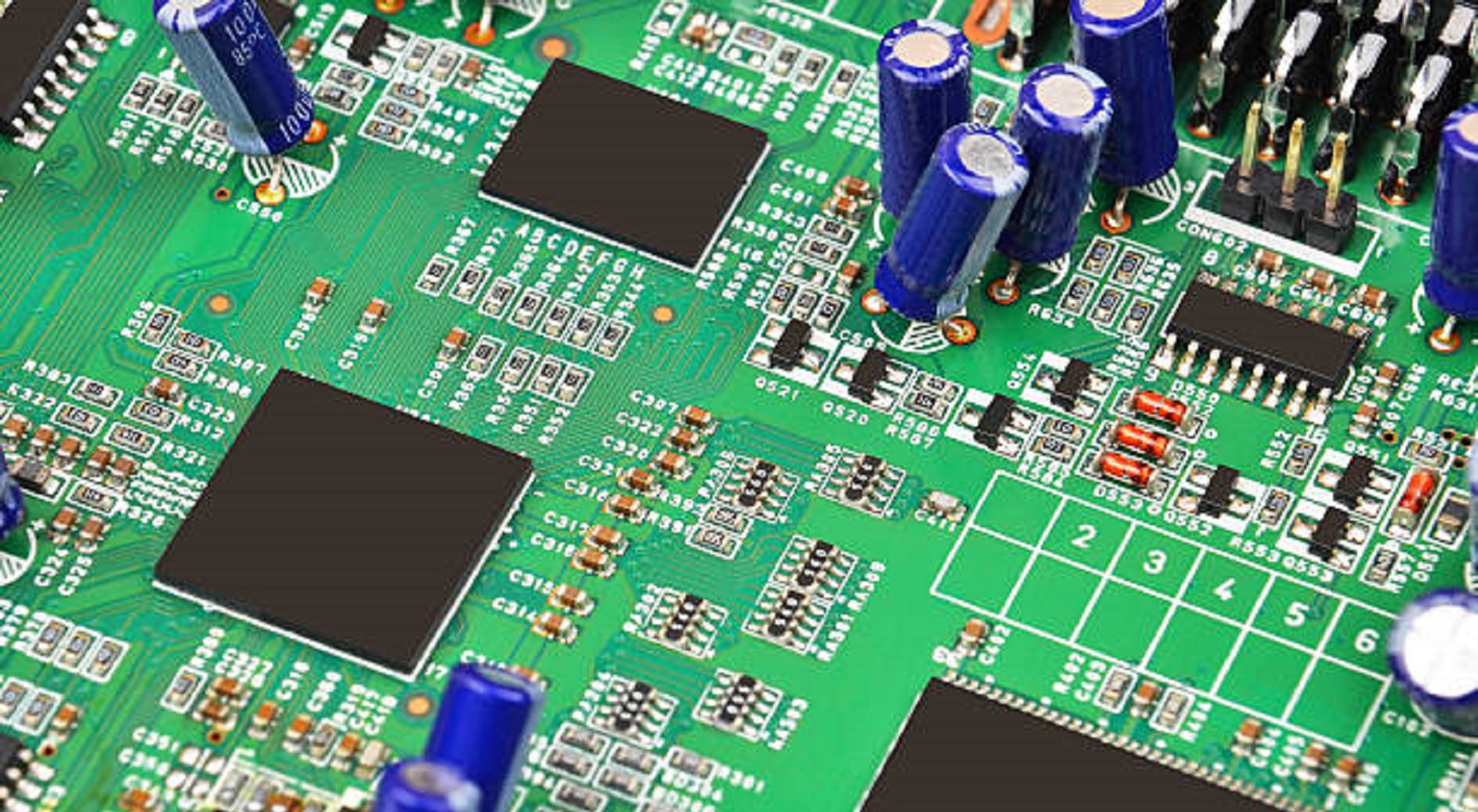
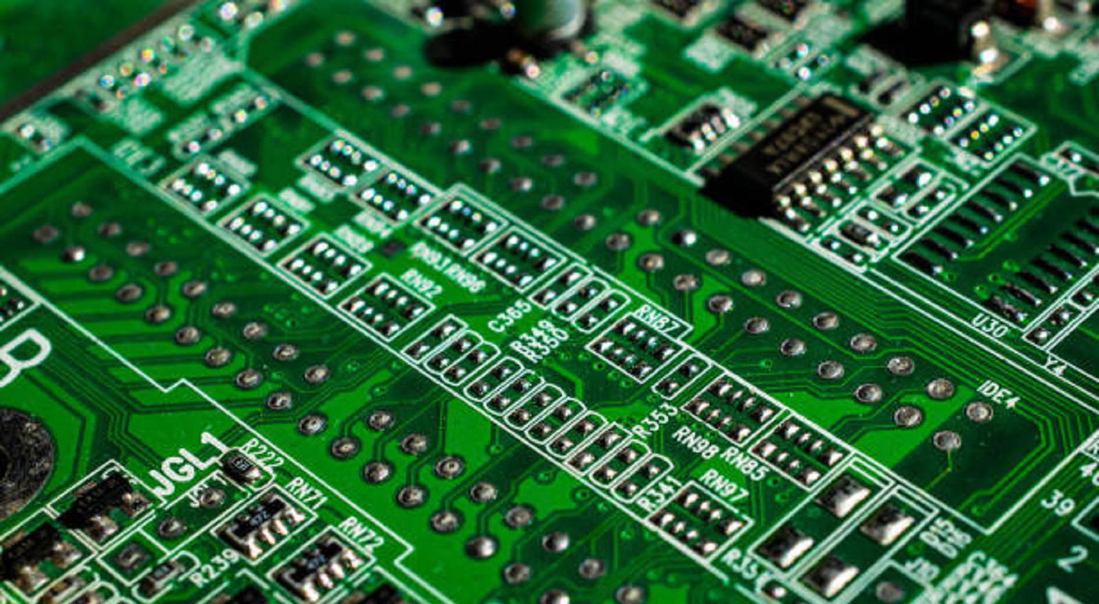
Printed Circuit Board routing is one of the most crucial phases in the design of Printed Circuit Boards, important since it bridges the theoretical schematic design to a realistic operational board. With the frontiers of electronic advancement shrinking into smaller, faster, and more complex dimensions, the need for keen, high-speed circuit pathways calls for professional routing techniques to ensure maximum performance and reliability. This comprehensive guide explores PCB routing, its significance, challenges faced by designers, best practices, and the tools that enhance the efficiency of the routing process.
What is PCB Routing?
Routing means delineating copper traces on a PCB to provide electrical connections among various components placed on it. It is the process that follows the placement phase, where the positions of the components are identified. It takes the circuit netlist derived from a schematic to a physical circuitry layout by connecting dots such that the electrical current can flow as intended.
The Importance of PCB Routing
Electrical Connectivity: Routing provides the backbone of interconnections between components on a PCB and is responsible for translating the logical schematic into a physical one, which is functional.
Signal Integrity: Effective routing helps in signal integrity by minimizing losses and preventing interference, critical for high-speed and sensitive circuits, where even minor disruptions can result in serious performance issues.
Thermal Management: Also, routing helps in the even distribution of heat by strategically planning the pathways, thus aiding in thermal management, which is vital for maintaining component performance and longevity.
Manufacturability: Good routing practices ensure that the PCB can be manufactured without issues, following DFM guidelines, which helps to minimize problems that can show up after production.
Challenges in PCB Routing
The routing of a PCB is like solving a big, complex puzzle, in which all the pieces need to connect efficiently within the constraints of space on the board. In this respect, there are several challenges faced by designers, such as:
High-Speed Requirements: The increase in the speed of circuits necessitates routing that will minimize impedance mismatches and crosstalk. This demands rigorous control of trace dimensions and separation, with proper applications of grounding.
Complexity of Design Rules: The designs nowadays require following strict design rules, especially for trace widths and spacings, and the implementation of vias, making routing more complex.
Component Density: Innovative routing is also needed to handle space and avoid interference in a signal due to more components found in small areas.
Shortened Design Cycles: The increasing demand for rapid prototyping puts pressure on designers to get the routing right the first time to avoid costly revisions and time-to-market delays.
Evolving Technologies: When new components and technologies are developed, designers are constantly updating the routing methodologies to adjust to new constraints and opportunities.
Best Practices in PCB Routing
In order to address these challenges, designers can follow a number of best practices:
Determine the Routing Strategy: First comes the routing strategy development considering the high-speed signal critical paths, bottlenecks, and optimization of signal path.
Layer Strategies: By using multiple layers strategically, one can employ dedicated power and ground planes to help improve signal integrity and reduce electromagnetic interference through stable reference levels.
Optimize Trace Geometry: Consistent trace widths and the avoidance of sharp angle turns will minimize signal reflections. Prefer rounded corners and smooth curves to reduce signal degradation.
Segregate Signal Types: Isolate analog and digital signal areas to avoid interference and achieve cleaner signal processing, which is essential in a mixed-signal environment.
Symmetrical Designs: Make the routing patterns balanced and symmetrical to improve the signal integrity and aesthetic appeal of the board layout.
Focus on Shorter Routes: Wherever possible, keeping traces as short as possible reduces potential losses and improves both speed and reliability.
Implement Differential Pairing: Controlled spacing differential pairs can be used where necessary-such as for high-speed digital signals-to greatly increase noise immunity.
Tools and Techniques for Effective PCB Routing
Advancements in CAD tools have greatly facilitated the process of PCB routing. The facilities and capabilities provided by them have eased the designer's effort in several ways:
Autorouting: Although these cannot replace the accuracy of manual routing, autorouting features in a tool like Altium Designer, KiCad, or Cadence Allegro will quickly route less-critical nets or at least provide a starting point for initial routing. Having parameters set correctly in advance pays off by making autorouting more efficient and reducing clean-up efforts.
Constraint Management: EDA tools with constraint managers enable designers to define and enforce trace spacing rules, trace width, impedance control, and many other key parameters in their designs. This ensures the adherence of design specifications throughout the routing process.
Simulation and Analysis: These signal integrity tools simulate the behavior of a circuit to preclude problems in crosstalk, timing errors, or power integrity for robust design performance before fabrication.
Inspection and Verification: Design Rule Checks will further ensure that the routed design meets the necessary specification and constraints, thus avoiding costly revisions post-manufacturing.
PCB routing is a very complex but very important part of the PCB design process, requiring a lot of skills, precision, and the use of sophisticated software. Following best practices supported by state-of-the-art routing technology, designers are able to address the challenges of today's modern electronics while ensuring their PCBs are both functional and manufacturable. Be it for amateur designers or professional ones, time spent on understanding and mastering how to route PCBs is always worth the effort since so much rests on it for the final performance, manufacturability, and reliability of a device. More crucially, embracing such insights into the working of these will be increasingly imperative as technology continues to advance.
Hot Tags:

Contact us

If you can't find what you're looking for, please contact us.
Article
Current limiting circuits are crucial in PCB designs, preventing overcurrent damage and ensuring safe, reliable operation across various electronic applications.
 2025/02/21
Effective PCB design ensures reliable electronics by optimizing component placement, connections, and testing, enhancing performance and longevity.
2024/10/31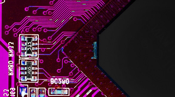
High-speed PCBs (>1GHz) are crucial for advanced electronics like 5G and data processors. Key practices include ensuring signal integrity, controlling EMI, and maintaining power integrity for reliable performance.
2024/09/27