- Products & Capabilities

- About
- Resources
PCBX.com Resources
Your source for industry knowledge, news, and expert insights

Latest Posts
Article

Learn how to apply DFA guidelines across PCB workflows from schematic to assembly, boost yield and cut production costs effectively.
 2026/05/26
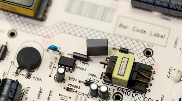
Learn core component lead forming techniques for axial & radial components, best practices, tools, and defect solutions to boost leaded assembly quality and production efficiency.
2026/04/14
Learn how to design mixed-signal PCBs with strong signal integrity using proven layout, grounding, and routing techniques for high-performance systems.
2026/04/09
Practical anti-ESD strategies for PCB design, including layer stack-up, layout, routing, component use and testing.
2026/04/02
Embedded electronics design focuses on small, low-power specialized computing systems, covering their classification, workflow, applications, benefits, challenges and future trends in modern tech.
2026/03/12
Proper trace-to-pad clearance in PCB design ensures safety, signal integrity, manufacturability, and longevity, following standards like IPC 2221 for optimal performance.
2026/01/29
PCB thickness is essential for device performance, impacting signal integrity, thermal efficiency, and durability, thus requiring careful selection for optimal outcomes.
2026/01/27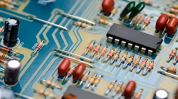
Understanding resistor power ratings in PCB design is crucial for ensuring circuit reliability, thermal efficiency, and preventing overheating through strategic layout and derating.
2026/01/15