- Products & Capabilities

- About
- Resources
PCBX.com Resources
Your source for industry knowledge, news, and expert insights

Latest Posts
Article
Learn proven PCB layout, grounding & stackup strategies to mitigate EMI, pass global EMC standards for high-speed electronics.
 2026/06/23
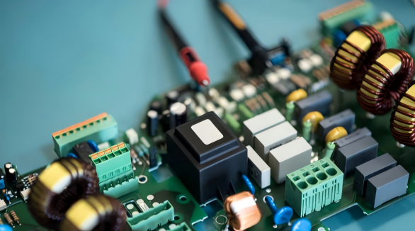
Explore critical creepage & clearance specifications for high voltage PCB design, including global standards and proven layout best practices.
2026/06/02
Proper trace-to-pad clearance in PCB design ensures safety, signal integrity, manufacturability, and longevity, following standards like IPC 2221 for optimal performance.
2026/01/29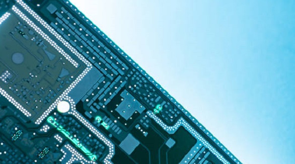
PCB routing is crucial for transforming schematics into functional layouts by ensuring electrical connectivity, signal integrity, and manufacturability amidst evolving design challenges.
2025/11/04
Optimize PCB layout for manufacturability by ensuring proper trace clearance, via placement, and incorporating testability features, while considering manufacturing tolerances.
2025/07/03
The article highlights the top 10 wireless router manufacturers, including Cisco, Netgear, and TP-Link, emphasizing their performance, features, and target markets.
2024/12/27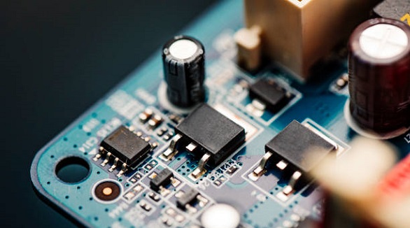
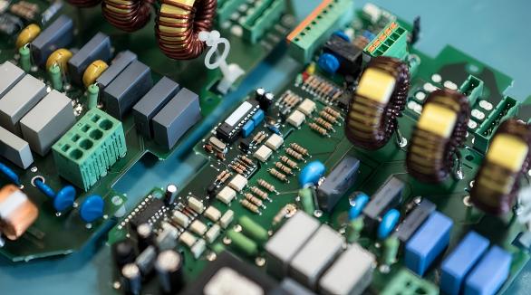
Effective power PCB design ensures high current handling, noise control, thermal management, and safety through specialized layout techniques and component selection.
2024/12/02
Motherboard PCBs connect key components, like CPUs and memory, in electronic devices. They require precise engineering and testing for optimal performance across consumer and industrial applications.
2024/10/11