- Products & Capabilities

- About
- Resources
PCBX.com Resources
Your source for industry knowledge, news, and expert insights

Latest Posts
Article

Explore effective solutions to minimize PCB ringing via impedance matching, routing optimization, component selection and pre-production testing.
 2026/06/11
Learn what PCB inner layers are, their types, functions, design rules, and common mistakes for reliable multilayer PCB design.
2026/06/09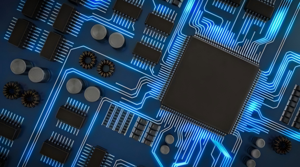
Learn what Chip-on-Board (COB) is in PCB design, covering types, manufacturing process, benefits and industrial applications for compact electronic circuit design.
2026/06/04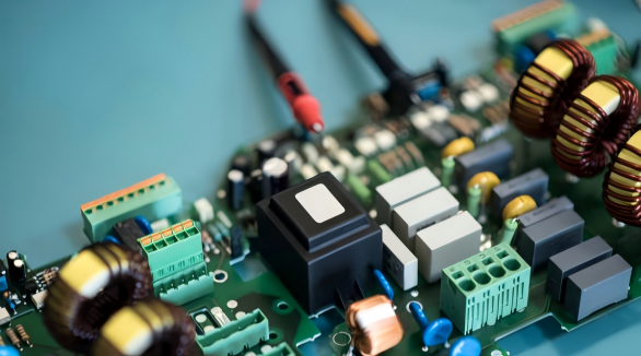
Explore critical creepage & clearance specifications for high voltage PCB design, including global standards and proven layout best practices.
2026/06/02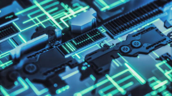
Learn how to apply DFA guidelines across PCB workflows from schematic to assembly, boost yield and cut production costs effectively.
2026/05/26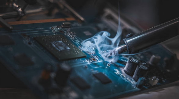
PCB trace repair guide with tools, methods, and tips to fix damaged circuit boards reliably.
2026/04/21
Learn how to design mixed-signal PCBs with strong signal integrity using proven layout, grounding, and routing techniques for high-performance systems.
2026/04/09