- Products & Capabilities

- About
- Resources
How to Reduce Ringing in PCB Design?


Explore effective solutions to minimize PCB ringing via impedance matching, routing optimization, component selection and pre-production testing.
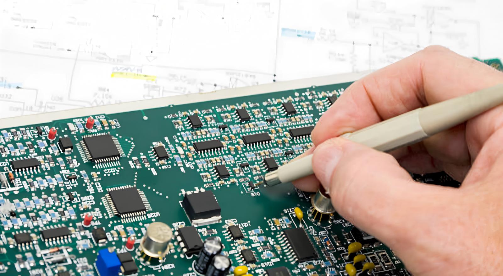
Ringing is a typical signal integrity issue in the design of a PCB, which refers to the unintended voltage oscillation that occurs when a digital signal transitions from low to high (or high to low). Often used as part of the high-speed clock lines, data traces, switching circuits. A high level of ringing may lead to incorrect logic triggering, increase electromagnetic interference (EMI), damage sensitive equipment and result in system failures. With the development of electronic products to higher speed and higher density, the control of ringing has become an important task for a reliable development of PCB. This article discusses the effects of ringing and provides practical and effective solutions, including circuit design, circuit layout, power management and material selection.
Fundamental Causes of PCB Ringing
The primary sources of ringing are reflection of the signal and parasitic resonance in the transmission lines. There is an inherent inductance and capacitance associated with a PCB trace. If the impedance of the signal source, trace and load are not equal, the signals reflect at the points where they are discontinuous. When incident wave and reflected wave are added together, voltage fluctuations come and go. There are many design defects that exacerbate this situation: excessive signal edges speed up the edges that contain rich high-frequency harmonics; long traces add more parasitic parameters; improper bends cause changes in the impedance; redundant stubs and broken ground planes also change the impedance and increase the chances of oscillation.
Comprehensive Strategies to Minimize Ringing
Use Precise Impedance Matching and Signal Termination
The simplest ways of reducing reflection and ringing are by impedance matching and terminating. There are two major termination methods that are applicable to various situations. The termination circuit for a series termination is a 22 Ω to 100 Ω resistor directly across the output pin of the driving chip. It is a suitable option for short and medium trace lengths, matches source and trace impedances, and is commonly employed with clock signals and digital I/O lines. Parallel termination is recommended for long single-ended traces. Add a pull-up or pull-down resistor in close proximity to the receiver whose resistance is equal to that of the trace characteristic impedance, which is normally 50 Ω, 75 Ω, or 100 Ω. If differential pairs such as LVDS are used, use a separate differential termination resistor near the receiving end. Be sure to keep all termination resistors close to chip pins, too much stub will add new parasitics and affect performance.
Moderately Adjust Signal Slew Rate
Another effective signal slew rate adjustment method is available. High frequency ringing can be easily excited by ultra fast rising and falling edges. The non-time-critical signals can have its signal edges smoothed appropriately. A 10pF to 100pF series ceramic capacitor is suitable for filtering high-frequency signals and smoothing out sharp edges on signal lines. The slew rate modes are programmable in most modern MCUs, FPGAs and logic chips. Slow slew rate can be used to reduce ringing without adding any additional components. But it is necessary to have moderate edge slowing. Too long of a transition time will result in timing errors and it will impact normal data communication.
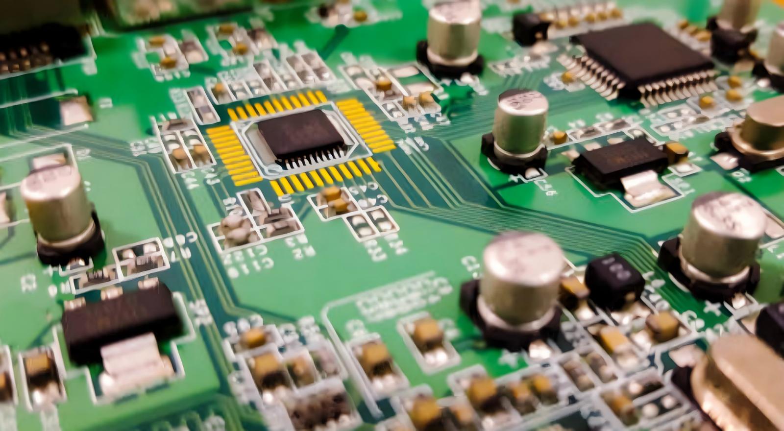
Implement PCB Layout and Routing Rules
Standardized layout and routing eliminate source ring. The first thing to do is to minimize the length of high-speed signal and clock paths and keep like components together. Secondly, prevent right angle bends and avoid unnecessary stubs on high speed paths. Instead use 45 degree or arc bends and keep trace width constant to keep impedance constant. Third, keep what is considered critical traces above a complete ground plane. A good reference plane not only optimises the signal return path but also reduces the parasitic inductance, crosstalk and keeps oscillations in check. Avoid putting high-speed traces near noise sources like power switches and inductors.
Minimize Grounding and Power Decoupling Design
Efficient distribution and grounding are also key factors. Create a decoupling network for all chips. Use the same polarity 0.1 μF high frequency capacitors as close to the power and ground pins as possible to suppress transient currents. Use small high-frequency capacitors and large bulk capacitors on large integrated circuits to deal with noise at various frequencies. Use thick copper traces/groups for ground and power lines instead of thin traces to reduce line impedance. In high-speed areas, beware of split ground planes since they will introduce longer return paths and make ringings worse. A simple RL snubber provides additional damping of parasitic resonance for switching circuits.
Choose the Right Components and PCB Materials
There is also a significant influence on the ringing performance of the composition of the components. If the device is performing as designed, use devices with moderate switching speeds rather than devices with very high switching speeds. Slower switching components will naturally have less high frequency harmonics and weaker ring. Use low jitter models for oscillators and clock sources for minimising initial signal distortion.
The quality of the high frequency signal transmissions depends on the PCB substrate materials. If you use high-speed, high-frequency designs, choose substrates with low dielectric-loss and low dispersion. High dielectric loss materials will cause distortion of signals at high frequencies, and worsen oscillation. In parallel, a reasonable design of the PCB stack-up: stack high-speed signal layer adjacent to ground layer to realize the accurate control of the impedance, so as to avoid mutual influence between high-speed signal layer and ground layer. Do not stack multiple high speed signal layers without ground isolation.
Leverage Simulation and Pre-Testing
Prior to mass production, take advantage of professional signal integrity simulation tools to test the amplitude of signal reflection and ringing, and trace impedance. Run various termination schemes, routing distances and component parameters to determine possible problems and design optimization before schematic and layout is finalized. Following prototype fabrication, measure real signal waveforms on oscilloscopes, confirm the improvement effect, and adjust component parameters and routing as needed based on the results of the oscilloscope test. Simulations and physical testing complement each other in the process of more effective, targeted ring control.
The choice of components and pcb can not be ignored. Use components that have a suitable switching speed rather than simply being after the fastest speed. Low jitter clock sources also contribute to clean original signals. To reduce the distortion of signals, choose low-dielectric-loss PCB substrates for high speed and high frequency applications. In the meantime, come up with a scientific "stack-up" by positioning high-speed signal layers adjacent to ground layers for stable impedance, and noise isolation.
Through the above comprehensive applications, designers can achieve significant reduction of signal ring, enhancement of signal quality, reduction of EMI risk, and ensuring long-term stable operation of electronic products. With continuously changing high-speed circuits, now it has become a fundamental skill for PCB engineers to learn about how to suppress ringing. With your trust in reliable, high-performance PCB design and signal integrity optimization services, PCBX is here to provide you with custom and top-notch solutions for your varying design needs.
Hot Tags:

Contact us

If you can't find what you're looking for, please contact us.
Article
PCB failures due to minor orientation and polarity errors can impact reliability, but proper design practices and checks ensure manufacturability and performance.
 2025/12/18
Castellated pads in PCB design facilitate easy board-to-board connections, enhancing miniaturization, assembly, solder quality, and flexibility for compact modules.
2025/01/13
Annular rings are crucial for reliable PCB electrical connections. Proper sizing, understanding issues like tangency and breakout, and best practices ensure optimal performance and reliability in electronic circuits.
2024/09/18