- Products & Capabilities

- About
- Resources
PCBX.com Resources
Your source for industry knowledge, news, and expert insights

Latest Posts
Article

Explore effective solutions to minimize PCB ringing via impedance matching, routing optimization, component selection and pre-production testing.
 2026/06/11
Nets in PCB design ensure logical connections from schematics to layout, enabling connectivity checks, design validation, and optimized manufacturing processes.
2024/12/05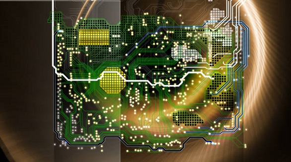
Power and ground planes in PCBs ensure signal integrity, manage heat, and minimize EMI, crucial for efficient, high-performance electronic devices.
2024/11/11
Tab routing in PCB manufacturing boosts efficiency and quality, ideal for non-linear shapes, offering flexibility, support, and cost-effectiveness in production.
2024/11/05
PCBX's new platform streamlines PCB design, offering real-time simulations, prototyping, and collaboration tools for students, hobbyists, and professionals.
2024/11/01
DFM ensures cost-effective PCB design by optimizing size, layers, materials, and components, focusing on manufacturability, reliability, and process efficiency.
2024/10/30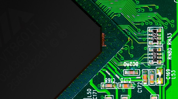
Tab routing enhances PCB production efficiency and quality, ideal for complex shapes. It offers cost-effectiveness, flexibility, and protection, crucial for high-precision designs and panelization.
2024/10/23
Designing PCBs for IoT demands innovation to tackle space, power, connectivity, and security challenges, ensuring robust, efficient, cost-effective devices that meet modern technological demands.
2024/10/18