- Products & Capabilities

- About
- Resources
PCBX.com Resources
Your source for industry knowledge, news, and expert insights

Latest Posts
Article
PCB Resources
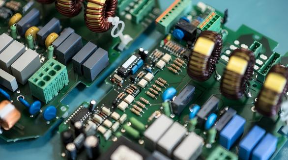
How to Effectively Control Electromagnetic Interference in PCB Designs
Learn proven PCB layout, grounding & stackup strategies to mitigate EMI, pass global EMC standards for high-speed electronics.
By PCBX 2026/06/23
2026/06/23
PCB Resources
How to Reduce Ringing in PCB Design?
Explore effective solutions to minimize PCB ringing via impedance matching, routing optimization, component selection and pre-production testing.
By PCBX2026/06/11
2026/06/11
PCB Resources
What Is an Inner Layer in PCB Design?
Learn what PCB inner layers are, their types, functions, design rules, and common mistakes for reliable multilayer PCB design.
By PCBX2026/06/09
2026/06/09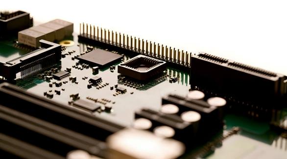
PCB Resources
Designing Mixed-Signal PCBs for Optimal Signal Integrity
Learn how to design mixed-signal PCBs with strong signal integrity using proven layout, grounding, and routing techniques for high-performance systems.
By PCBX2026/04/09
2026/04/09
PCB Resources
Common Mistakes to Avoid in PCB Layout
Optimize PCB layout for manufacturability by ensuring proper trace clearance, via placement, and incorporating testability features, while considering manufacturing tolerances.
By PCBX2025/07/03
2025/07/03