- Products & Capabilities

- About
- Resources
What Is an Inner Layer in PCB Design?


Learn what PCB inner layers are, their types, functions, design rules, and common mistakes for reliable multilayer PCB design.
Today, all modern electronic devices are carried in a printed circuit board (PCB). While single-layer or double-layer PCBs can be used to make simple electronic modules, multilayer PCBs are used in more compact, fast, and precise electronics like smartphones, industrial control units, and communication devices. In the stacked structure of multilayer PCBs, the inner layers constitute the core components of a circuit, thus affecting its performance, stability and compactness. This article elaborates on the definition, classification, core functions, standard design guidelines and common design pitfalls of PCB inner layers, helping designers grasp the basic logic of multilayer PCB design.
Basic Definition of PCB Inner Layers
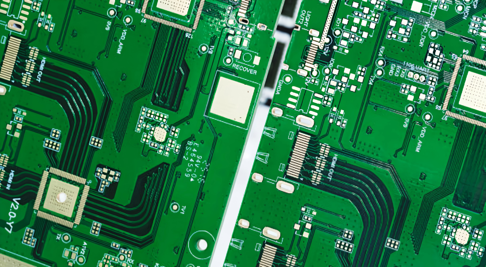
The concept of multilayer PCB is a multi-layered sandwich structure that consists of a series of conductive copper layer and insulating FR4 dielectric materials to avoid short circuits in the circuit. All PCB layers have been separated in to outer and inner layers. The upper and lower exposed copper layers are referred to as outer layers, and primarily used for components soldering or surface signal transmission. All the copper layers that are sandwiched between the two outer layers are the inner layers.
Inner layers are tightly laminated during PCB manufacturing process, which will be completely isolated from outside environment and can't be directly observed and operated. The number of inner layers can vary with the complexity of the design. The 2-layer and 2-internal layers PCB is the most commonly used, and it is the most suitable PCB for beginner multilayer designing. When high density wiring or high frequency circuits are needed, 6-layer, 8-layer or more inner layers are necessary to meet the performance and space requirements.
Main Types and Working Principles of Inner Layers
From the functional point of view, the PCB inner layers are mainly classified into inner signal layers and inner power/ground planes, which work together to ensure the circuit system is able to operate normally.
Inner signal layers are additional routing space for electronic signals. They effectively solve the problem of outer layer wiring congestion and are specially applicable to laying high-speed signals like clock signals and data transmission signals. Typically, designers take steps to control the impedance on inner signal layers, which can drastically minimize crosstalk, reflection and EMC (electromagnetic interference) and enhance general signal integrity.
Inner power and ground planes are paved with a continuous copper area covering, instead of the signal layer traces. The ground plane supplies the zero potential reference for the circuit throughout and also establishes a low impedance return path for the current, which helps to eliminate circuit noise. The power plane is used to distribute power to ensure stable voltage to prevent load voltage drop and provide continuous and stable power for components. For conventional stackup, power plane and ground plane provide natural electromagnetic shielding for the signal layers.
Also, vias are crucial for an inner layer's operation. Vias act as conductive connecting holes to provide electrical conductivity between the layers and between the outer layers and components, and to complete the cross-layer signal and power transmission.
Core Value and Advantages of Inner Layers
Modern PCBs have become popularized inner layers, which allows for miniaturization and a high performance. They are the first to bring the improved space utilization. The outer layers have less space for more complex wiring needs and the inner layers offer additional wiring area for compact circuit design.
Secondly, inner layers ensure the best electrical efficiency. Matching design of the power and ground planes will significantly minimize circuit impedances and noise, essential requirements for stable operation of high frequency circuits (>100MHz). Thirdly, the large area copper layer of the inner layers has excellent thermal conductivity, so that the thermal energy generated by high-power components can be rapidly dissipated, and then the stability and service life of the board can be improved. The totally enclosed inner layers, however, prevent erosion of dust and moisture, further helping to increase the reliability of PCBs over time.
Basic Design Specifications and Common Mistakes
The 4 layer PCB is the most approachable and convenient design for the novice designer and consists of two signal layers, a ground layer and a power layer. This topology is good for minimizing loop inductance and maximizing signal transmission efficiency. Designers must ensure that all copper surfaces of power planes and ground planes are completely covered, minimize the number of breaks in the power and ground planes, and by using an arc or a 135-degree trace, rather than a right angle, to connect devices, will reduce signal loss. Also, vias should be placed reasonably, meaning that several vias are placed in a region of high current to decrease the resistance, and the number of vias is minimized in high-speed signals to prevent signal delay.
However, some common design pitfalls need to be avoided. If too many splits are made on power and ground planes, then the current return path will be compromised and there will be more electromagnetic noise. If the signal can't be controlled by impedance, excessive use of vias will cause the signal to be distorted and structural defects to occur. Furthermore, if there is no thermal relief pads for via connection, it will impact the yield and quality of the assembly.
Inner layers are the invisible backbone of multilayer PCBs, undertaking core functions such as wiring expansion, power distribution, noise reduction and heat dissipation. Reasonable inner layer design directly determines the signal integrity, stability and service life of the entire circuit system. Mastering inner layer design rules is a basic skill for every professional PCB designer. For high-precision and standardized multilayer PCB production and customized inner layer design solutions, PCBX can provide professional PCB manufacturing service, including one-stop technical support and high-quality assembly and fabrication services to ensure your PCB design is perfectly presented in actual production.
Hot Tags:

Contact us

If you can't find what you're looking for, please contact us.
Article

4-layer PCBs optimize space, performance, and cost, making them ideal for electronics requiring reliable and compact designs, such as in consumer electronics, telecom, and automotive.
 2025/11/20
FR4 permittivity affects PCB signal speed and impedance. It's crucial for design, requiring careful management in high-frequency applications for reliability.
2024/12/16
Choose between single-layer or multi-layer PCBs based on your project's needs. Single-layer is simpler and cost-effective; multi-layer offers complex functionality and durability. Evaluate based on functionality, size, durability, budget, and turnaround time.
2024/08/05