- Products & Capabilities

- About
- Resources
Balanced Copper Distribution and Copper Weight in PCBs


Learn PCB copper weight standards & balanced copper distribution rules to avoid warpage and boost board stability for electronic design.
Printed circuit boards (PCBs) serve as the backbone of modern electronic systems, making and breaking connections, carrying signals and distributing power. There are several parameters that contribute to the quality of a PCB, two of which are important enough to mention as prerequisites for mechanical stability, electrical performance, manufacturability and long-term reliability: balanced copper distribution and copper weight. They are usually discussed independently, but they really go hand in hand to determine the performance of a PCB under the actual operating and manufacturing conditions. This article will provide insight into their fundamental definitions, real-world implications, design principles, and how they work together to facilitate strong PCB design.
What Is Copper Weight and Why Is It Important?
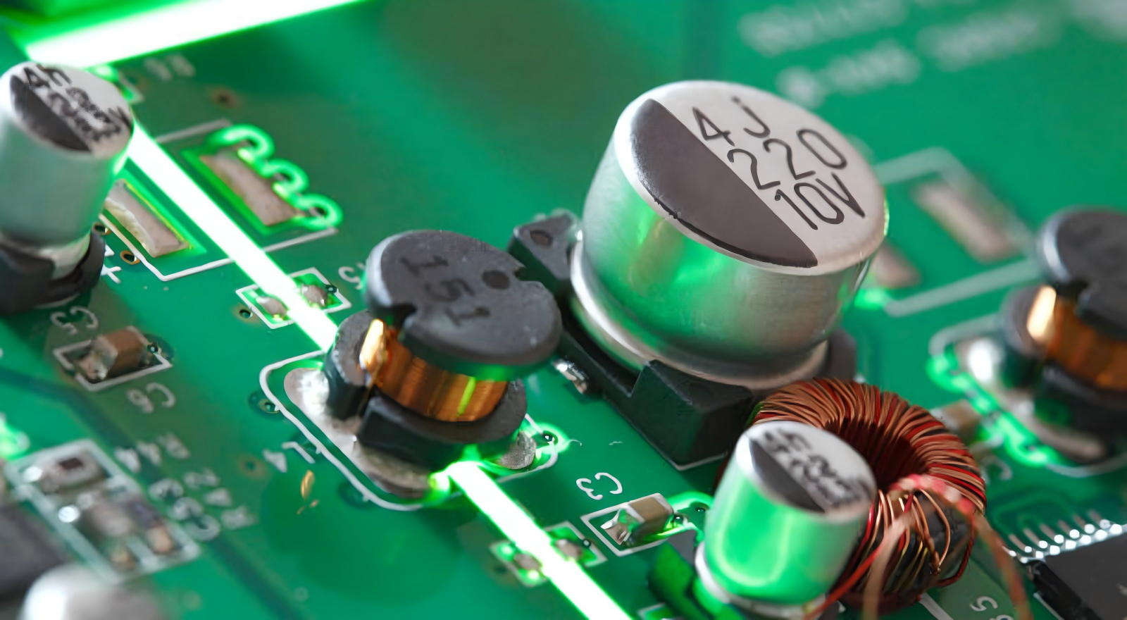
Copper weight refers to the amount of copper foil used on a PCB layer, and is expressed in ounces of copper per square foot (oz/ft2). One ounce of copper uniformly spread over one square foot equals a nominal thickness of about 1.37 mils (approximately 34.8 μm). The current carrying capacity, thermal dissipation and mechanical strength of the board is directly specified by this specification.
The following are a few examples of the various types and applications of standard copper weights:
0.5 oz (~17 μm): Fine traces and tight spaces require this in high density interconnect (HDI) boards in inner layers.
1 oz (~35 μm): This is the typical thickness used for most general-purpose electronics, which offers a compromise between cost, etchability and performance.
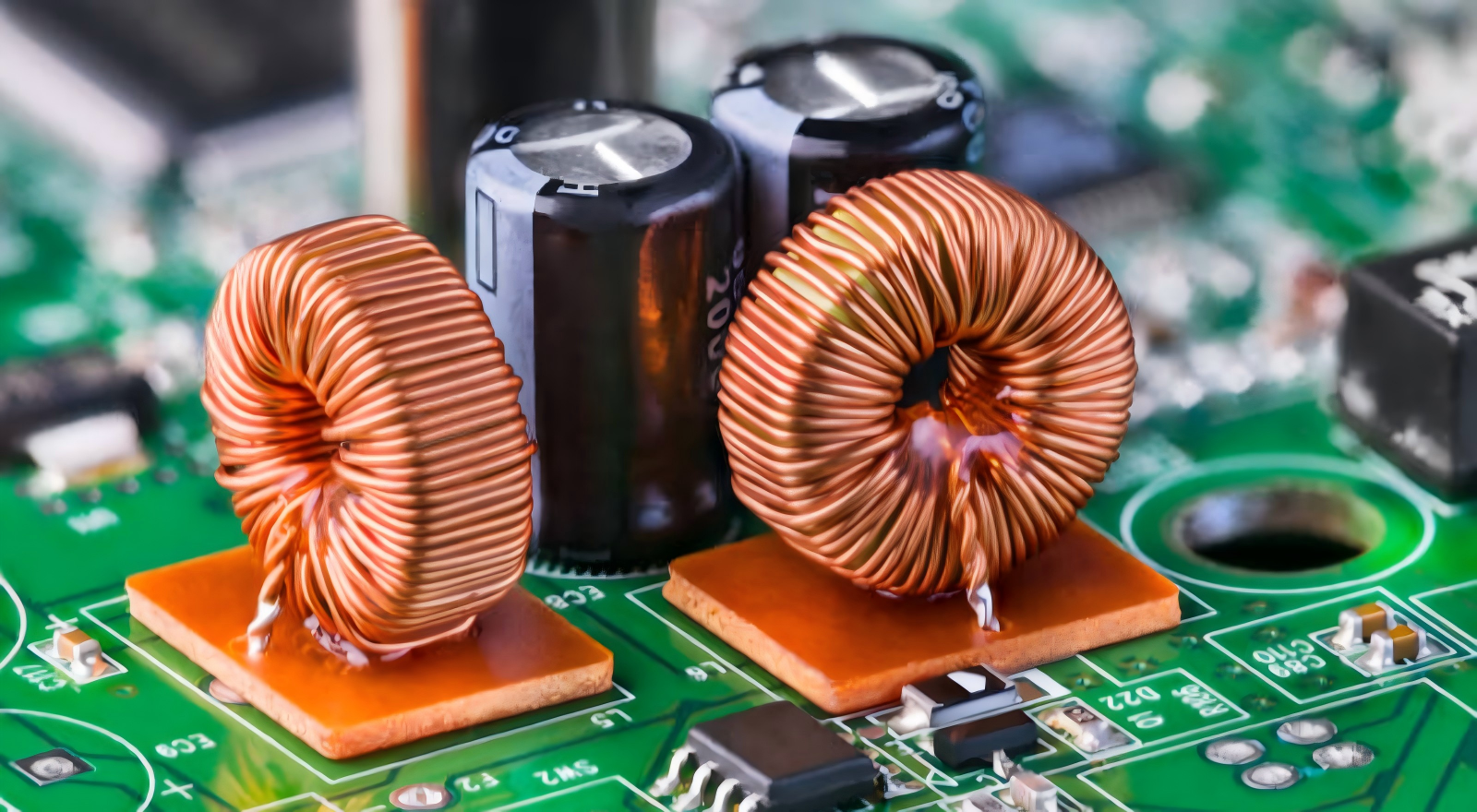
2 oz (~70 μm): Recommended for power paths, LED drivers, medium power circuits, and when higher current and heat spreading is required.
Heavy copper (3 oz and above 105 μm+): Industrial Controls, Power Converter, Auto Controls, and high reliability equipment.
The heavy copper results in a lower resistance, lower voltage drop, higher thermal conductance, and higher current density. But it also calls for extra meticulous manufacturing control, such as longer etching times and wider trace spacing, to prevent electrical shorting and plating defects.
Balanced Copper Distribution: Mechanical and Process Stability Key
Balanced copper distribution indicates even distribution throughout the entire distribution layer (even coverage for all layers) and even copper density between the two layers of a layer stack (symmetry between paired layers). The primary objective is to reduce any internal stress that can result from the difference in the coefficient of thermal expansion (CTE) for copper and the dielectric material, such as FR‑4.
Differential density of copper causes differential expansion and contraction in high and low copper density areas during lamination, soldering and thermal cycling. This imbalance causes stresses, which result in common failures:
Warpage, Bow and Twist: Structural deformations which impede assembly and component placement.
Delamination/Blistering: Separation between layers / formation of bubbles that reduces the strength of the board.
Uneven Plating/Etching: Over etching in the sparse areas and under etching in the dense areas – Trace defects and unreliable connection.
Resin Voids: These are voids that form during the lamination process because of the differential pressure of lamination, which decrease insulation and structural integrity.
According to IPC‑6012, the maximum allowable bow and twist is 0.75% for SMT‑assembled boards and 1.5% for non‑SMT boards. These limits may only be respected with a balanced distribution, particularly for high reliability IPC Class 3 applications.
How to Achieve Balanced Copper Distribution
Uniform copper throughout the board can be achieved through the use of practical design techniques:
Symmetrical Layer Stack-up: Design the stack-up from the center outwards and mirror layers for a design to ensure copper and dielectric thickness balance.
Copper Thieving: Generate nonfunctional copper shapes in low density areas for plating current balancing and for preventing uneven etching.
Cross‑hatched Copper Planes: Use mesh patterns for cross hatched copper planes for better resin bonding, mechanical stress reduction, and impedance control.
Uniform Trace Layout: Do not bunch up too many copper traces on one layer; spread out the traces across the layer.
Copper Filling: Open areas that require balancing of coverage between opposite layers fills with solid or mesh copper.
Thicker Board Cores: If you need a higher degree of rigidity and less risk of warping, use boards with a thickness of ≥1 mm.
The Synergy between Copper Weight and Balanced Distribution
Copper weight and balanced distribution are correlated. For these thicker copper layers, more consideration must be paid to the distribution of stress. On the other hand, a well-balanced layout can optimize the use of any copper weight, by providing even current distribution, heat distribution, and quality of the plating.
Lighter Copper (0.5-1 oz) is used for high speed designs to provide a level of precision in controlling impedance. Balanced layout minimizes crosstalk and signal skew for high speed designs. Heavy Copper (2-4 oz) for power electronics gives high current handling and symmetry reduces thermal fatigue and structural failure.
Design Best Practices
Compare the weight of copper to current, thermal and density requirements.
Care should be taken to keep the stack-up symmetrical, even for cores and prepregs.
Balance low density areas with thieving and hatching.
Adhere to IPC standards for width, spacing and warpage limits.
Run a DFM check and/ or a thermal cycling test to validate designs.
Work with manufacturers to meet process capabilities.
Copper distribution and weight is not a frivolous feature, it's a critical element of PCB performance and reliability. Copper weight determines the amount of current and heat a board can realistically carry, and balanced distribution provides mechanical stability and manufacturability by keeping the board from warping, delaminating, or having improperly formed traces. Together, they enable PCBs to meet the demands of consumer, industrial, automotive, and high‑reliability systems.
Understanding these principles is crucial for designers and engineers striving to create robust and production-ready boards. By careful planning, symmetrical layout and an appropriate choice of copper, failures can be reduced, costs reduced and time to market speeded up.
PCBX helps customers achieve these objectives through superior guidance in design, dependable manufacturing services, and the expertise to ensure that your projects are balanced copper distribution and optimal copper weight.
Hot Tags:

Contact us

If you can't find what you're looking for, please contact us.
Article
Copper weight determines PCB effectiveness in conductivity, thermal management, and mechanical strength, essential for high performance in various applications.
 2025/08/12
Copper balance is key in PCB fabrication, ensuring signal integrity, thermal management, and reliability by managing copper distribution for efficiency.
2025/08/07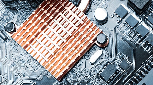
Aluminum PCBs offer cost-effective thermal management for moderate applications, while copper PCBs excel in high-performance electrical and thermal tasks.
2024/12/20