- Products & Capabilities

- About
- Resources
Lifted Pad and Issues on Printed Circuit Boards


Lifted pads disrupt PCB performance due to thermal and mechanical stress. Solutions involve better design, materials, and handling to ensure reliability.
In an age of technology, Printed Circuit Boards (PCBs) are inevitable, the structural and functional heart of millions of electronic products. PCBs interconnect electronic components through conductive paths, known as traces, and cover a vast range of applications from small devices to complex aerospace systems. But among the typical issues that may compromise the performance of PCBs is the case of "lifted pads." This article covers causes, implications, and remedies of lifted pads, demystifying prevention methods and repair methods in the PCB manufa cturing industry.
Understanding the Role of Pads in PCBs
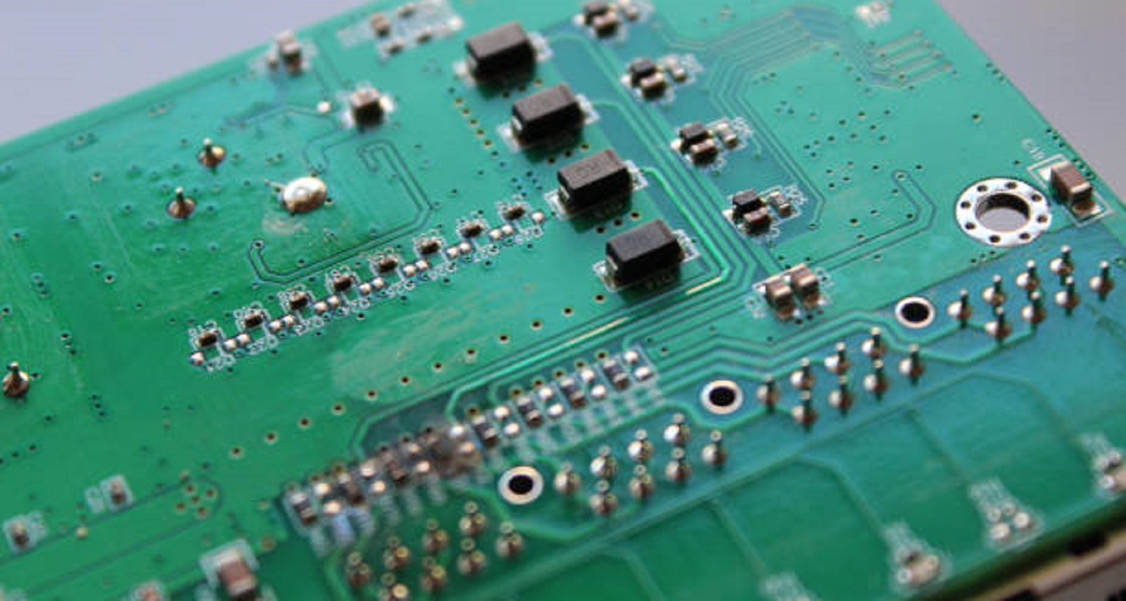
PCB pads are small conductive surfaces manufactured to facilitate the connection of component pins to copper paths. Pads function as the soldering interface for components and allow electrical connection within circuitry. If a PCB has lifted pads—a condition where such surfaces become separated from the PCB's laminate—it can severely impair the board's operation up to a level of intermittent or complete loss of electrical connection.
Reasons for Lifted Pads
Thermal Stress: High thermal exposure, especially during assembly, is one of the primary causes for lifted pads. Techniques like wave soldering yield high temperatures, especially for single-layered PCBs, which can lead to diminished copper bonding and thus pad lifting. When pads are subjected to improper temperatures, their adhesion with the PCB substrate diminishes, and they lift easily due to succeeding thermal or mechanical stress.
Mechanical Stresses: Improper handling and application of excessive mechanical stress can enhance the possibility of pad lifting. During soldering or component installation, when excessive pressure is applied, it can lead to pad detaching. These stresses are especially problematic during rework or repair processes when one needs to avoid loosening weak connections.
Material Quality and Adhesion: Material quality used in the construction of PCB plays a major role in determining pad integrity. Thermal-resistant adhesives with poor quality or poor thermal resistance can fail when exposed to heat, causing lifted pads. Additionally, the material characteristics should be compatible with the operational environment of the board to guarantee long-term reliability.
Design and Manufacturing No-nos: Inadequate pad design, such as improper size or misalignment, usually results in pad lifting during assembly. Adhering to industry standards like IPC-7351 becomes the necessity, making pads suitable to bear both through-hole and surface-mount technology without compromising structural integrity.
Effects of Lifted Pads on PCBs
The effect of lifted pads can have far-reaching implications on PCB reliability and performance:
Interruption in Connectivity: Lifting of pads equates to broken circuits, leading to poor or failed electrical contacts. Lifting may lead to erratic failure of devices, significantly affecting device performance and user satisfaction.
Rises in Operating Expenses: Additional time and labor are involved to diagnose and repair lifted pads, raising operating costs. Such operations also tend to include partial or complete dis-assembly, thus tending to make the operation logistically demanding.
Reliability and Longevity Problems: PCBs with faulty pads produce products that fail repeatedly, damage brand reputation, and generate unhappy customers. In safety-critical applications such as in medical or aerospace technology, such failures would have disastrous consequences.
Prevention Steps to Prevent Lifted Pads
Pad lifting prevention entails holistic design, material selection, and assembly process measures:
Improved Thermal Management: Choose adhesive materials or epoxies that have high thermal resistance to ensure pad adhesion even under high thermal stress. Adding heat sinks or thermal pads can offer further thermal dissipation, keeping the board in its best temperature condition during operation.
Best Practice Handling and Assembly Procedures: Implement stringent handling procedures to avoid mechanical stress on components. Handle boards carefully while soldering, and avoid oversized components that apply too much pressure on the pads.
Utilization of Through-Hole Technology: Using through-hole technology can enhance pad and component strength, greatly minimizing the likelihood of pad lifting. Through-hole designs provide stronger mechanical connections, particularly useful in high-stress or high-vibration applications.
Industry Standard Compliance: Utilizing industry standards like IPC-7351 guarantees correct pad sizing and layout, eliminating the possibility of errors that lead to weakness or inconsistency in pad stability. Using design software that features library generators streamlines pad design, reducing the risk of human error and meeting industry best practices.
Repairing Lifted Pads: Is It Worth?
Repairing raised pads can be a complexity, and whether a PCB should be repaired or replaced is determined by various factors:
Trace Repair Methods: In minor lift issues, connecting thin wires to by-pass faulty traces can restore contact. Though a time-consuming process, this method keeps the original PCB and is cheap compared to replacement of an entire board.
Reattachment with Epoxy Adhesives: Pads may be reclaimed with high-strength epoxies. It is a method that is exact and can be tried if the working environment of the board will not subject it to excessive future stress.
Component Reorientation: Altering component orientation to allow better alignment and attaching the pads may prevent further lifting, thus creating stable connections in the short term.
Vendor Assessment: When recurring pad lifting problems occur, there may be a need to assess the existing PCB vendor. Recurring faults could be signs of poor processes or materials and may require switching to better methods to enhance the quality of products.
Lifted pads pose a serious issue in PCB fabrication but with embracing strategic design and manufacturing practices, their effect can be minimized. By precise thermal management, proper handling procedures, proper utilization of through-hole construction, and following industry standards, manufacturers can improve PCB reliability and customer satisfaction. With PCBs increasingly becoming more complex and more application-oriented, constant innovation in assembly technology and materials is imperative to address the issue of lifted pads, helping electronic devices attain the high levels of expectation for today's consumer and industries in general.
Hot Tags:

Contact us

If you can't find what you're looking for, please contact us.
Article
Rigorous PCB inspections using AI, AOI, and X-ray technology ensure high quality, reduce costs, and enhance efficiency in electronics manufacturing.
 2025/04/10
PCB pads connect components on circuit boards. Understanding through-hole, surface-mount, and BGA pads is key for effective PCB design and manufacturing.
2024/11/08
PCB repair skills reduce waste and costs, ensuring durable electronic functionality by effectively diagnosing and fixing various board failures.
2024/10/25