- Products & Capabilities

- About
- Resources
Optimizing PCB Performance with Copper Pour


Learn professional copper pour techniques to boost PCB signal integrity, reduce EMI, improve thermal management, and ensure reliable manufacturing.
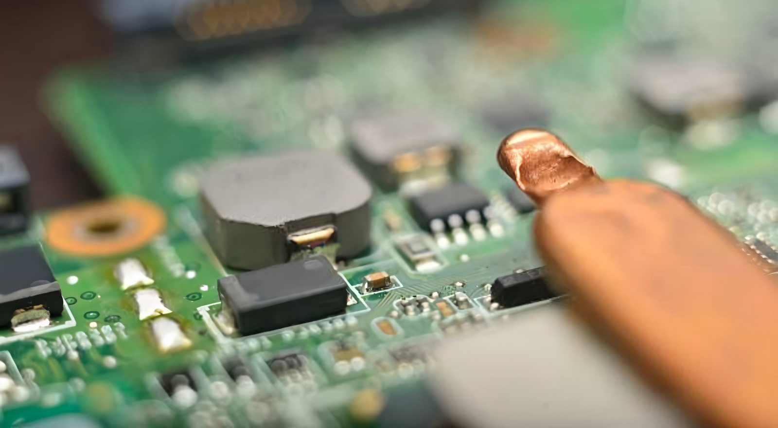
Copper pour in contemporary PCB design is much more than a cosmetic fill; it is a foundational engineering practice that has a direct impact on signal integrity, power stability, EMI/EMC compliance, thermal control, and manufacturing reliability. Copper pour that is inadequately done causes noise and manufacturing issues, when done correctly, it turns unused board space into high performance infrastructure to high-speed high-power and miniaturized electronic systems. This guide covers essential principles, techniques, and best practices to enable you to deploy copper pour with accuracy, which will result in maximum performance in all design applications.
Core Purpose of Copper Pour: More than Spacefilling
Copper pour is a method of filling unrouted PCB areas with solid or hatched copper, generally grounded or power-net connected. Its worth increases with the frequency of circuits beyond 100 MHz and power densities, which are key issues that compromises performance. Effective copper pour designs provide four transformative advantages:
Improved Signal Integrity: The continuous ground plane reduces the area of signal return current loops, which reduces jitter, reflection and distortion, which are important to the reliability of data transmission in high-speed circuits.
EMI Suppression: It acts as a distributed shield, preventing radiated interference and containment of switching noise, with emissions of 1020 dB lower and requiring less FCC and CE compliance (or CISPR).
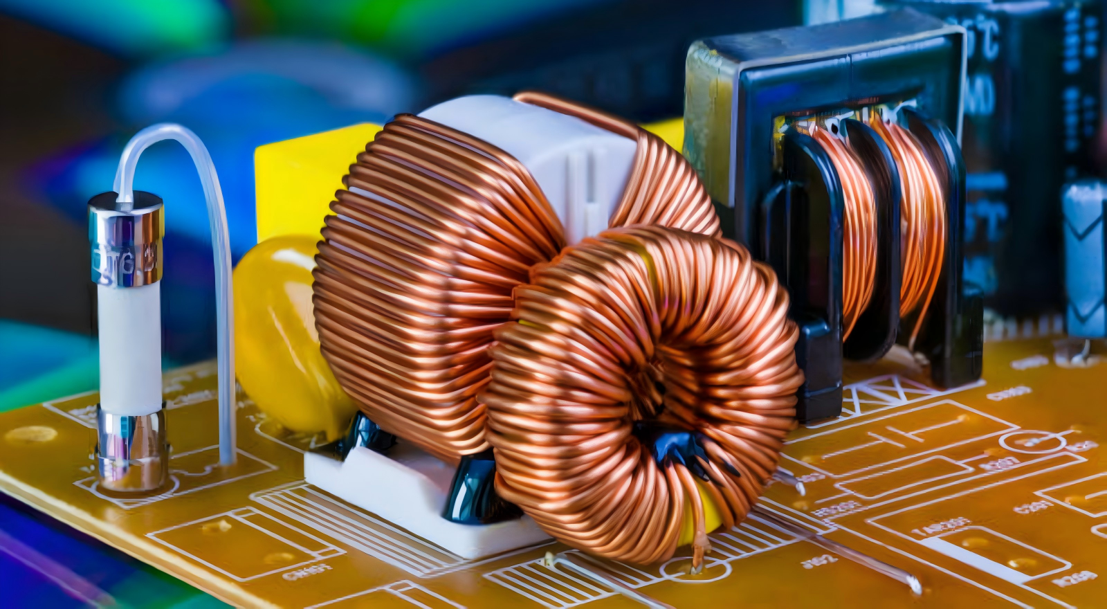
Stable Power Distribution: It offers low resistance circuits to carry power, reducing voltage drops. Copper plane A 1 oz/ft2 can safely carry 10 A with little loss, and special power planes ensure voltage rails are stabilized at sensitive components.
Efficient Thermal Control: With copper having a high thermal conductivity, it can easily absorb the heat produced by power semiconductors and regulators, reducing maximum temperatures and increasing component life.
Core Design Principles for Optimum Performance
Pouring copper involves more than automated pouring, it needs to be planned. The best results are based on four major techniques:
Hardened Ground Planes: The EMI Backbone
Give preference to solid continuous ground planes in multilayer designs. Assign ground the entire internal layers, and tie the top/bottom pours to internal layers with stitching vias to ensure even shielding. One should avoid excessive splits of the planes - this forms high-impedance return paths and increases noise and signal distortion. Solid ground plane minimizes EMI by as much as 20 dB, and is therefore a non-negotiable requirement in high-frequency designs (above 500 MHz).
Efficient Power Planes to Clean Power
Design your own power planes to meet the needs of your circuit. High-current paths should be done in copper, 2 oz/ft2 or more, to avoid overheating. Separate voltage domains (e.g., 3.3 V, 5 V) to avoid cross-domain noise coupling, and place decoupling capacitors within 1 mm of IC power pins. Use short traces or vias to connect these capacitors to power and ground planes in order to reduce inductance, and provide stable power to sensitive electronics.
Via Stitching: Layered Shielding & Stability
Via stitching joins copper pours across layers, boosting shielding effectiveness and reducing impedance. Stitching vias of space at a frequency of around λ/20 th of the maximum operating frequency (e.g. 15 mm at 1 GHz) to prevent resonance. Install vias at the edges of the board and high-speed/RF circuit to create a protective shield against EMI. For high-current paths, use multiple vias in parallel to lower resistance and enhance reliability.
Balanced Copper Distribution: Eliminating Warpage
Lack of uniform copper density leads to PCB warping, etching imbalances and assembly stress. Target an increase or decrease in copper density by 1015% on a per-layer basis. Most designs should be done with solid pours- hatched (grid) pours are only applicable in exceptional cases such as manual soldering. Add small copper “thieves” (balancing shapes) to equalize distribution, ensuring uniform etching and mechanical stability.
Best Practices & Critical Design Rules
These IPC-compliant rules will help prevent expensive mistakes and achieve manufacturability:
Clearance Rules: Have at least 0.2 mm (8 mil) between pours and traces/pads in low-voltage circuit designs and 0.5 mm (20 mil) in high-voltage designs; and 0.5 to 1.0 mm between board edges and pours to avoid delamination.
Thermal Reliefs: Pads when soldering on large pours use four symmetric 45° spokes, which connect to a large pad in order to avoid cold solder joints and tombstoning.
Eliminate Floating Copper: Turn on the setting of design tools to remove unconnected copper islands, which are unintentional antennas and negatively impact EMC performance.
Shape Optimization: Round internal corners (radius no less than 0.5 mm) so that no acid traps occur during etching; no small copper necks that can be broken under thermal or mechanical stress.
Application-Specific Tuning
Tailor copper pour to your design’s unique needs:
High-Speed Digital: Have continuous ground planes on critical traces; do not route signals across split planes. Minimise crosstalk by up to 30% by pouring ground between signal traces.
Analog & RF: Use distinct analog and digital grounds, and put them together at one point near the power input, to prevent ground loops. Apply grounded copper pour around sensitive traces, becoming grounded at only one end.
Power Electronics: High-current layers should use 2-3 oz/ft2 copper and thermal vias should be paired with power device pours to effectively remove heat.
Mixed-Signal: Divide the board into analog, digital, power regions, and separate ground pours which are linked at a single star ground point around the main power connector.
Common Pitfalls to Avoid
Splits Due to Air Traffic: Unintended, interrupting return paths, causing noise and signal jitter. Keep splits to a minimum, use copper bridges where required.
Omitting DRC Checks: Clearances that are not verified cause shorts, solder bridging and scrap. Check Run Design Rule Checks (DRC) with each change of pour.
Sharp Internal Corners: Lead to acid trapping and over-etching. Enhance manufacturability by using rounded corners.
Inequal Distribution of Copper Density: Causes warping and uneven etching. Density of the balance on all layers.
Failure to use Thermal Reliefs: Causes solder defects. Always have thermal spokes on standard pads attached to large pours.
Copper pour is a high-impact practice that brings PCB performance to a new level, making it not only functional but also excellent. With solid ground planes, balanced copper distribution, and application specific tuning, you turn empty board space into a strategic resource. By following the industry guidelines and common traps, high signal integrity, low EMI, and effective thermal management can be achieved, as well as manufacturability that is predictable even in hard-to-manufacture applications.
When it comes to professional design, advanced DFM analysis, and high-quality PCB production to actualize your optimized copper pour designs, rely on PCBX—your preferred partner in high-performance and reliability.
Hot Tags:

Contact us

If you can't find what you're looking for, please contact us.
Article
Copper weight determines PCB effectiveness in conductivity, thermal management, and mechanical strength, essential for high performance in various applications.
 2025/08/12
Copper balance is key in PCB fabrication, ensuring signal integrity, thermal management, and reliability by managing copper distribution for efficiency.
2025/08/07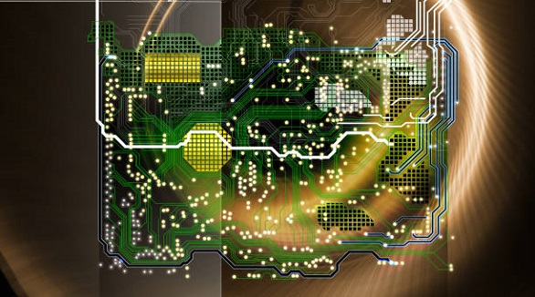
Power and ground planes in PCBs ensure signal integrity, manage heat, and minimize EMI, crucial for efficient, high-performance electronic devices.
2024/11/11