- Products & Capabilities

- About
- Resources
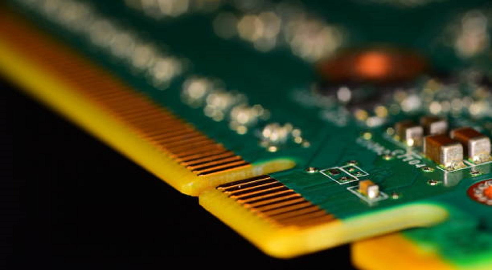
PCB Edge Plating


PCB edge plating enhances connectivity, mechanical strength, EMC, and thermal management, crucial for diverse sectors, with trends toward higher density and durability.
Innovation is very important to address the ever-growing demands for compact, efficient, and durable PCBs. This field has introduced the process of PCB edge plating among many other innovations at the forefront of research. At PCBX, we value the critical impact this process contributes to improving functionality and reliability for PCBs in various industries.
Understanding PCB Edge Plating
Also known as PCB edge connector plating, it involves the deposition of a conducting metal layer, usually copper, gold, or tin, along the exposed edges of a PCB. It may be done on single-layer, double-layer, and multilayer boards to enhance mechanical and electrical properties of such boards for applications in devices that require reliable connectivity through edge-mounted connectors.
Key Benefits of PCB Edge Plating
Improved Connectivity: Edge plating offers a uniform conductive path; this is necessary in applications with edge connectors. It presents a reliable connection, especially in those devices that require signal integrity, including servers, expansion cards, and new communication equipment. The plated edges provide great contact areas for the edge connectors, thus guaranteeing ease in integration and at the same time ensuring minimal signal loss.
Improved Mechanical Strength: Edge plating significantly reinforces the edges of the PCB, especially for enhancing its mechanical robustness. This is very useful in applications with mechanical stress and with frequent insertions/ withdrawals, which reduces the risk of edge damage or board failure during handling and operation. This additional layer of metal enhances the structural integrity of the board by reinforcing the material to prevent damage from potential occurrences throughout the assembly and use.
Superior Electromagnetic Compatibility: The metal layers laid down during edge plating serve as an effective electromagnetic shield that assists in the reduction of EMI emissions from the board while protecting it from external electromagnetic noise. This would be important for signal integrity in sensitive electronic environments. Therefore, superior EMC is increasingly critical for today's modern electronics, where a number of components are fitted within a small area, necessitating increased shielding.
Better thermal management: Due to the ever-increasing amount of components that generate heat on modern PCBs, managing temperatures effectively is becoming increasingly important. Edge plating helps enhance thermal conductivity and allows better dissipation of heat generated from the board, which helps in high-density or high-power applications where temperature regulation is at the heart of maintaining performance and longevity.
Aesthetic Enhancement: Beyond functional benefits, edge plating gives a clean, professional finish to PCBs, thereby enhancing the aesthetic appeal of these boards. This is very important in consumer electronics and other products where the looks provide the additional perceived value. Sleek, metallic edges improve durability but also help visually in the product's overall appeal.
Challenges and Considerations in Edge Plating
While the advantages of edge plating are obvious, there are a number of technical issues that need to be addressed in order to maximize this advantage. The added cost and additional design complexity of edge plating must be carefully balanced against its advantage. Design and manufacturing processes need to be very precise to avoid short circuits arising from unwanted metal bridging.
The selection of the proper material for plating will make the board compatible with the usage environment. Manufacturing should be left to a partner with experience and appropriate technology that can deliver quality edge plating. This is important in cost management to achieve the right balance between performance and durability.
Diverse Applications Across Industries
Edge plating of a PCB finds applications across various sectors where durable and reliable board connections are essential. In the telecom sector, edge plating is crucial for router cards, base stations, and switching cards. In computing, it enables the connection of servers and allows backplanes and expansion cards to handle high-frequency data.
The automotive industry relies on edge-plated PCBs for robust engine control units and instrument clusters, while in military and aerospace, they are utilized in mission systems and navigation cards. Medical fields use them in higher-order imaging equipment such as MRI and ultrasound machines. Ease of accessibility and versatility also make edge plating a favorite in consumer electronics, especially when immediate field replacements are required for products such as set-top boxes and game consoles.
Future Trends in PCB Edge Plating
As electronic devices continuously improve, so does the field of edge plating technology. Emerging trends are toward increasing the contact density on thinner boards to permit more complex interconnections. Driven by demand for faster data transmission, there is a continuing push to implement high-frequency signal integrity at data transmission rates greater than 10 Gbps with advanced plating techniques.
Improvements in durability are underway as well, with innovative plating techniques designed to withstand over 10,000 mating cycles. Cost-efficient manufacturing processes have gone through much refining to make edge plating more accessible across all industries. This ensures that the field of edge plating will always be one of the cornerstones of modern PCB design and manufacture and can help the electronics industry fulfill its drive toward innovation.

In essence, edge plating on a PCB is the fundamental process around which durability, connectivity, and performance needs are centered in modern electronic devices. Significantly improving the mechanical and electrical properties of PCBs, edge plating provides engineers with a means to meet the demanding expectations of today's technology-driven world. While this process introduces further considerations in design and manufacturing, the benefits it offers make it an indispensable tool for developing robust, reliable electronic products. At PCBX, we are committed to leading in this field-innovating solutions that adapt to the challenges of modern electronics. As the pursuit of innovation continues, PCB edge plating will remain integral to the advancement of electronic engineering and design, sustaining relevance far into the future.
Hot Tags:

Contact us

If you can't find what you're looking for, please contact us.
Article
PCB edge mounting optimizes space, enhances modularity, and improves connectivity by placing connectors on board edges, aiding in flexible, efficient system design.
 2024/12/11
PCB copper plating is key for creating conductive traces that drive electronic circuits, offering benefits like conductivity, anti-corrosion, and cost-effectiveness. Plating methods include electroless and electrolytic.
2024/09/25
Etching is crucial in PCB production, removing unwanted copper to create conductive pathways. Techniques include chemical, laser, plasma, and photochemical etching, each with advantages and limitations ensuring PCB performance and reliability.
2024/09/24