- Products & Capabilities

- About
- Resources
How to Effectively Control Electromagnetic Interference in PCB Designs


Learn proven PCB layout, grounding & stackup strategies to mitigate EMI, pass global EMC standards for high-speed electronics.
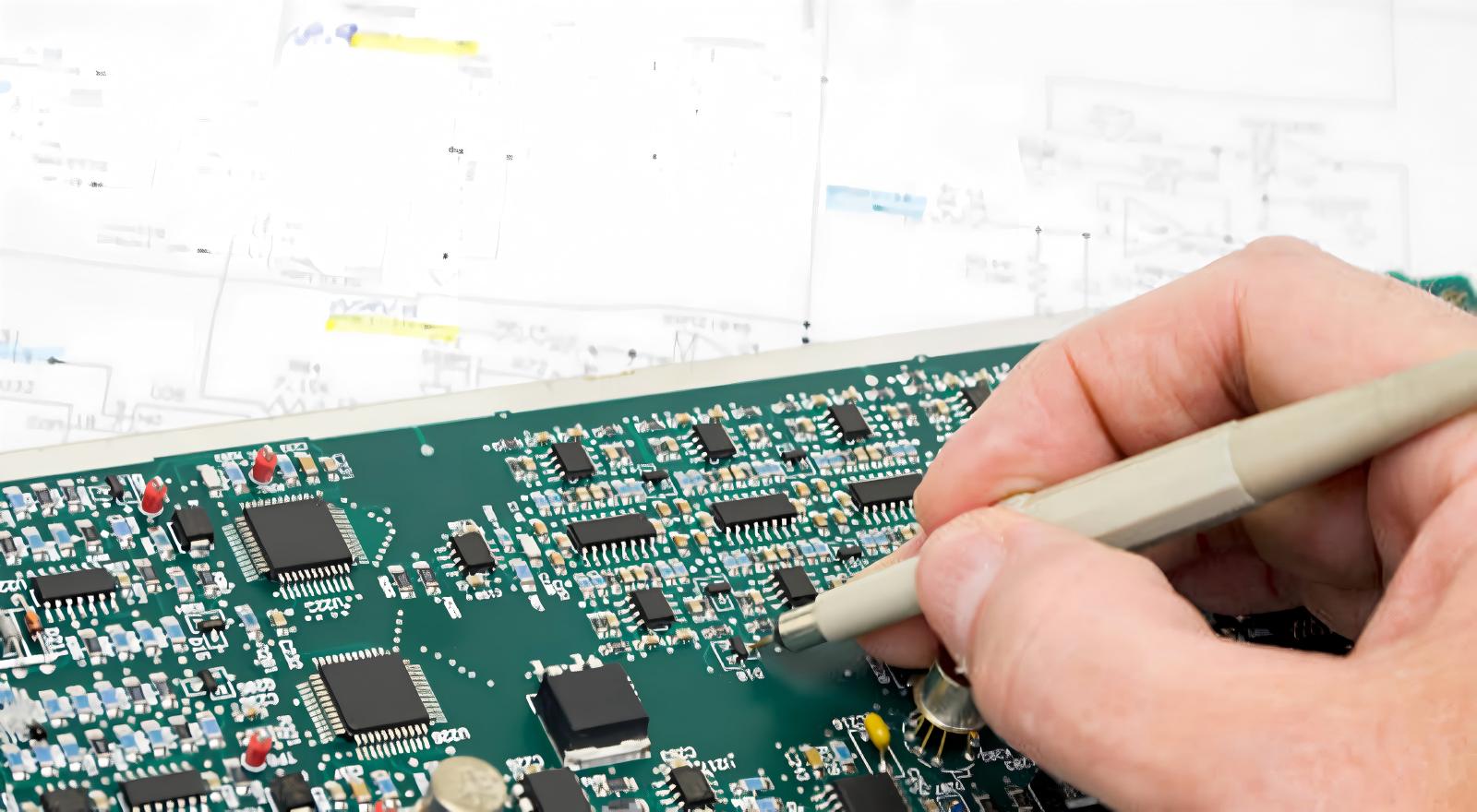
Electromagnetic Interference (EMI) is one of the most difficult and un-negotiable problems in today's circuit design due to the continuous trend of electronic miniaturization, high-speed signal transmission and dense integration of PCB. EMI: Unwanted electromagnetic noise created by high speed switching circuits, power modules, clock signals that spoils the integrity of internal signals and disrupt the normal operation of neighboring electronic equipment. Electromagnetic Compatibility (EMC) on the other hand refers to the ability of a device to operate without causing significant radiation or susceptibility in a complex electromagnetic environment. There are many demanding international regulations for industrial, automotive, medical and consumer electronics products such as FCC, IEC or CISPR standards. If no EMI control measures are taken scientifically at design time, engineers are likely to experience prototype test failures, multiple board revisions, higher costs and delayed product deliveries. The only way to create effective EMI management is to optimize your PCB design processes proactively and consistently, without resorting to post-production shielding and filtering techniques. The article goes in-depth on the basic EMI mechanisms and high-efficiency mitigation strategies used in today's PCB designs.
Core Root Causes of PCB EMI
The majority of the problems of electromagnetic interference (EMI) with PCB are because of unreasonable current return paths and distributed transmission line effects. The typical low-frequency lumped circuits produce no perceptible EMI noise because the length of the traces are far shorter than the wave length of the signal. Almost every modern high-speed PCBs use distributed circuit systems, however. When the signal rise time is very short, and the trace length is also long, the characteristics of ordinary PCB traces will transform into these unexpected antenna structures, resulting in signal reflection, waveform ringing, crosstalk, continuous electromagnetic radiation and so on.
Based on the basic principle of electromagnetism, the current of a signal creates a closed circuit with a forward trace current and return current, which always takes the path of least inductance. The area of the current loop is proportional to the intensity of the radiation from EMI. The outer layer microstrip traces emit electromagnetic radiation and radiate in the open air, clearly. Incomplete and split ground planes result in return currents having to pass through loop areas which are much greater than normal, creating intense radiation sources along the "slots". When it comes to real-life tests, the majority of EMC failures are from common-mode noise, which is produced by unbalanced differential traces and ground potential inconsistencies, rather than from conventional differential-mode noise.
Key EMI Mitigation Layout Practices
Component Selection and Functional Zoning
The selection of the components is at the heart of low-EMI PCB design and needs to be done with care. In cases of selection of equivalent functional chips, designers should select the chips whose ground and reference pins are evenly spaced. This type of packaging enables lower inductance and shorter return paths for neighboring signal pins, thereby limiting inter-pin noise coupling. On the other hand, high-frequency decoupling capacitors need to be located near the power pins of the IC to reduce switching noise, and bulk capacitors with larger capacitance values are needed to smooth out low-frequency power supply ripples.
The most economical means of EMI isolation is functional zoning. The designers must divide the PCB into different zones of noise sources and signal areas. Precision analog sensors, weak-signal amplifiers and sampling circuits are considered as highly sensitive modules, on the other hand high-speed logic chips, clock oscillators and switching power units are regarded as centralized noise sources. Different zones are physically isolated 20 times the trace-to-plane height by a professional design rule to prevent magnetic field coupling. Tightly grouped interconnected components reduce signal traces and prevent distributed line radiation, and physical separation is always better than ground plane separation when it comes to noise suppression.
Stackup, Grounding and High-Speed Routing
The best structure for suppressing EMI in multi-layer PCBs is an integrated and complete reference plane. Embedded stripline routing allows electromagnetic fields to be localized within the dielectric medium, thus confining the field to the dielectric layer, making it appropriate for high speed differential signals, clock signals, and RF circuits. Outer-layer microstrip routing is only recommended for low-speed control lines because there will be unavoidable field leakage. Optimizing return current paths and further reducing loop inductance by reducing the dielectric thickness between signal traces and ground planes to less than 8 mils.
Ground planes are not allowed to be split under high-speed traces. In the case of mixed analog and digital design, a single complete ground plane is used with local physical zoning while a single-point star grounding is used to eliminate ground potential difference. Dense ground stitching vias will effectively reduce high frequency plane resonance and field leakage. If signal vias penetrate multiple reference layers, we must also add matched grounding vias to ensure low-impedance return paths around these signal vias. Furthermore, to minimize crosstalk, designers need to adhere to the traditional 3W routing guideline: keep the traces differential in length as short and as tightly coupled as possible; avoid long parallel traces and right-angle bends that result in impedance discontinuity.
Supplementary Shielding and Filtering Design
Physical shielding and passive filtering are important auxiliary measures for those products that have ultra-strict EMC requirements and are required for high precision and high frequency applications. The metal shielding type can be used to wrap the modules with strong electromagnetic radiation, providing electromagnetic radiation shielding and magnetic radiation protection for the inside of the module. Finally, ferrite beads and LC filter networks placed on external connectors may provide excellent filtering of high frequency common mode conducted noise, providing stable and standard compliant signal output.
Common Pitfalls and Compliance Verification
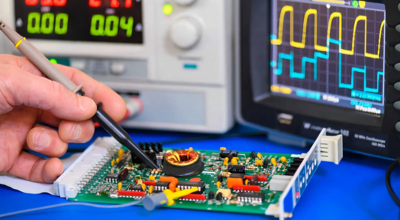
Typical EMI design issues are placement of decoupling components, lack of stitching vias, unreasonable splitting of the ground plane and mismatching of differential pairs. These small layout issues will cause serious radiation over-limit issues in formal EMC testing. The EMI design flow method is a standardized method which involves pre-layout simulation risk assessment, post-layout electromagnetic field analysis and prototype chamber testing based on FCC and IEC standards. With iterative optimization using test data, expensive board redesigns can be avoided.
EMI management in PCB design is a systematic engineering work focusing on source suppression and path optimization. By optimizing the return loop, standardizing the design of the grounding stackup and with the correct scientific layout zoning, electromagnetic radiation and signal crosstalk can be significantly reduced. As electronic product performance continues to improve, the ability to prevent or eliminate EMI has become a major part of the PCB development process and is now essential for creating a high-quality PCB. Professional technical support is required for engineers who are interested in the circuit design with reliability, stability and EMC. PCBX is a trusted PCB solution provider, providing customized stackup design, high-speed layout optimization and EMI verification services to help global customers quickly resolve electromagnetic compatibility issues, and to shorten the time for mass production of products.
Hot Tags:

Contact us

If you can't find what you're looking for, please contact us.
Article

Signal reflection in PCBs, due to impedance mismatches, can be managed with impedance matching, termination methods, and strategic layout to ensure reliability.
 2025/09/09
Voltage regulator PCBs ensure stable electronic device operation, offering solutions like linear and switching regulators for efficiency and reliability in designs.
2025/01/10
Power and ground planes in PCBs ensure signal integrity, manage heat, and minimize EMI, crucial for efficient, high-performance electronic devices.
2024/11/11