
- Products & Capabilities

- About
- Resources
PCB Layout and Routing Rules for Reliable Board Design


Key PCB routing rules for trace width, impedance control, via placement, plane integrity, and testability — practical guidance for reliable board design.
Routing decisions made at the layout stage determine far more than whether a board looks tidy — they set the ceiling for signal integrity, thermal performance, EMI compliance, and manufacturability long before the board reaches assembly. Routing discipline is what keeps first-pass yield high and rework low, regardless of how complex or tightly scheduled a program is. This article consolidates the routing rules that consistently separate boards that assemble and test cleanly from those that generate field returns or ICT failures.
Trace Width and Current Capacity
Trace width must be sized to the current it carries, not simply drawn to a comfortable default. Undersized traces develop excessive temperature rise, which accelerates copper fatigue and, in dense layouts, can degrade adjacent components. IPC-2152 provides current-carrying capacity guidance based on trace width, copper weight, layer position (internal vs. external), and permissible temperature rise, and should be the reference standard rather than rule-of-thumb charts carried over from earlier designs. Power and ground traces, in particular, warrant explicit calculation rather than visual estimation, since these nets often carry the highest sustained currents on the board.
Controlled Impedance for High-Speed Signals
Any net carrying high-speed digital or RF signals — differential pairs, clock lines, serial interfaces — needs impedance control rather than arbitrary trace geometry. Impedance is a function of trace width, copper thickness, dielectric height, and dielectric constant, so it must be calculated against the actual stack-up rather than assumed. Differential pairs additionally require length matching and consistent spacing along their full length to preserve edge timing and minimize skew. Deviating from the target impedance — even locally, such as at a via transition or connector breakout — introduces reflections that show up as eye-diagram degradation or intermittent link errors during test.
Via Placement and Structure
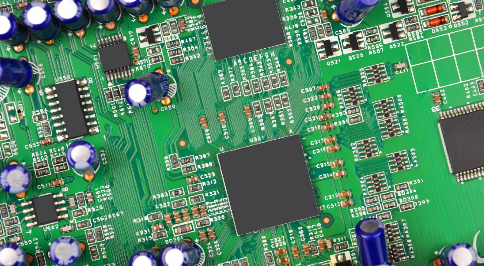
Vias are discontinuities, and every via on a high-speed or high-current path should be placed deliberately rather than wherever routing convenience dictates. On high-speed nets, minimize via count on critical signals, and where a layer transition is unavoidable, place a nearby ground via to provide a return path and reduce the discontinuity's impact. For high-current nets, a single via is often insufficient; multiple vias in parallel reduce both resistive loss and thermal concentration. Via-in-pad on BGA and fine-pitch footprints should be filled and capped per the fabricator's process, since an unfilled via under a pad can trap flux or solder during reflow and lead to voiding.
Ground and Power Plane Integrity
Solid, unbroken reference planes are one of the most effective and most frequently compromised routing disciplines. Signal traces routed across plane splits or through cutouts lose their continuous return path, which raises loop inductance and radiated emissions. Where a plane split is unavoidable — for example, between analog and digital power domains — critical signals should not cross it; if crossing is unavoidable, a stitching capacitor near the crossing point can provide a local return path. Digital and analog ground pours should generally connect at a single, deliberate point rather than being left to merge incidentally in the copper pour.
Component Placement Before Routing
Routing quality is largely determined before the first trace is drawn. Placement should group functional blocks — power conversion, high-speed digital, sensitive analog front-end — so that routing between them stays short and predictable, and so that noisy switching regulators sit physically away from sensitive analog or RF sections. Decoupling capacitors need to sit as close as physically possible to the IC power pins they serve, with a direct, low-inductance connection rather than a shared via or long stub. Placement decisions that ignore routing consequences tend to force compromises later — sharp trace angles, long return paths, or unavoidable plane crossings — that are difficult to correct without a layout rework cycle.
Spacing, Creepage, and Clearance
Trace-to-trace and trace-to-plane spacing must satisfy both electrical clearance requirements and the fabricator's process capability. IPC-2221 clearance tables, referenced against operating voltage, altitude, and conformal coating status, are the appropriate starting point rather than a blanket minimum carried from a previous, lower-voltage design. For boards with mixed high-voltage and low-voltage sections — common in industrial power and test equipment — creepage and clearance at the boundary between domains deserves particular attention, since this is where insulation coordination failures typically originate.
Routing for Testability
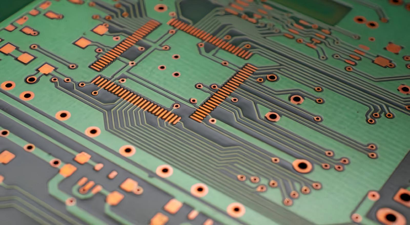
Routing choices affect test coverage as much as they affect signal performance. Nets intended for in-circuit test (ICT) or flying-probe access need a reachable test point on an accessible layer, placed with enough surrounding clearance for the probe. Routing a net entirely on an inner layer with no via breakout to an accessible surface removes it from ICT coverage, forcing reliance on functional test alone to catch defects on that net. Coordinating routing with the test strategy early — rather than retrofitting test points after layout is complete — keeps test coverage and layout density from working against each other.
Thermal Relief and Copper Pour Considerations
Copper pours connected to through-hole pads should use thermal relief spokes rather than solid connections, since a solid connection acts as a heat sink during soldering and can prevent the joint from reaching reflow or wave temperature. The spoke count and width should still be sufficient to carry the intended current for power and ground connections — thermal relief is a soldering accommodation, not a license to under-size the connection. On boards with heavy copper power layers, coordinating relief geometry with the assembly process avoids trading one defect mode (cold joints) for another (undersized current paths).
PCB routing rules exist because they encode failure modes that are expensive to diagnose after the board is built — signal reflections, thermal fatigue, EMI non-compliance, untestable nets. Applying them consistently, and treating placement as part of the routing decision rather than a separate step, keeps boards moving cleanly from layout through assembly and test and keeps first-pass yield predictable across builds.
At PCBX, our engineering team reviews incoming designs against these routing disciplines during DFM analysis, flagging impedance, clearance, and testability issues before they reach the assembly floor. If you're preparing a design for production, contact our team for a DFM review ahead of your build.
Hot Tags:

Contact us

If you can't find what you're looking for, please contact us.
Article
Learn how to design mixed-signal PCBs with strong signal integrity using proven layout, grounding, and routing techniques for high-performance systems.
 2026/04/09
PCB failures due to minor orientation and polarity errors can impact reliability, but proper design practices and checks ensure manufacturability and performance.
2025/12/18
Optimize PCB layout for manufacturability by ensuring proper trace clearance, via placement, and incorporating testability features, while considering manufacturing tolerances.
2025/07/03