
4、Schematic Edito
4.1 Project Design Flowchart
Figure 4-1
4.2 Schematic (SCH) Design
After creating a project in PCBX, it automatically redirects to the SCH editing interface (For an introduction to the workbench, see section 3.1)
4.3 SCH Design - Menu Bar
In the drop-down of the first left item icon of the menu bar,you can return to the Workbench home page, or return to the PCBX official website home page。

Figure 4-2
4.3.1 File Menu
The File Menu includes:Save、Save as、Close、Import、Export Wizard、Export PDF。(Figure 4-3)
Save:Save the current content within the SCH (schematic) project (Shortcut Key:Ctrl + S)
Save as:Save a copy of the project file with a new project name。(Figure 4-4)
Close:Close the current project and return to the workbench homepage。
Import:Import KiCad、Altium Designer、Eagle files。
Export Wizard:Options to export project SCH, PCB, symbol libraries, footprint libraries, and BOM (Bill of Materials)。(Figure 4-5)
Export PDF:Option to export the project's schematic and BOM (Bill of Materials) in PDF forma。

Figure 4-3
Figure 4-4

Figure 4-5
4.3.2 Edit Menu
Select:Select any element in the SCH editing interface. Hold down the Ctrl + left mouse button for multiple element selection. You can also hold the left mouse button to box select elements. Box selection can be divided into right box selection or left box:
 Select to the right: the color of the border is blue, and only the elements completely selected within the box can be selected (all elements are included)
 When box-selecting to the left, the border color is grey, and elements are selected if they are partially included within the selection box (partial element inclusion)
 ;
;
Rotate:Rotate the selected component symbol, rotate right (shortcut key R), rotate left (shortcut key E)。
Delete :Delete the selected element, or press the Delete key on the keyboard。
Copy: Copy the selected elements (shortcut key Ctrl + C)。
Paste :Paste the last copied elements (shortcut key Ctrl + V). When pasting components, the reference designator will automatically increment by one。
Mirror:Mirror the selected elements along the X (horizontal) axis. (Shortcut key Shift + Y) Mirror the selected elements along the Y (vertical) axis (Shortcut key Shift + X) 。
Undo:Undo the previous action, reverting to the last state step (Shortcut key Ctrl + Z) 。
Redo:Redo the functionality of the last or multiple undone actions(Shortcut key Ctrl + Y) 。
Figure 4-6
Align:Alignment functionality for multiple elements/components is available:
Alignment can be done to the left, right, top, bottom, horizontally centered, and vertically centered, as well as horizontal and vertical distribution。
Taking Figure 4-7 as an example, after selecting the component symbols R1, R2, and R3 and executing a left align, the alignment will be based on the leftmost element (R1) as the reference object for the left alignment (see Figure 4-8). The right, top, and bottom alignment functions work similarly to the left alignment, using the element closest to the alignment direction as the reference object for alignment。
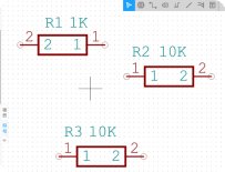
Figure 4-7
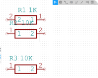
Figure 4-8
Alignment horizontal center : Horizontal center with the leftmost element as the reference object。
Alignment vertical centering : Vertical centering with the top side element as the reference object。
Horizontal distribution: Adjusts the selected elements to have equal horizontal spacing (left to right) without changing their vertical positions。
Vertical distribution: Adjusts the selected elements to have equal vertical spacing (up and down) without changing their horizontal positions。
After Select Edit-Align-Align...;the 'Align Objects' window pops up (see Figure 4-9), where you can perform alignment operations simultaneously in both horizontal and vertical directions for the selected elements。
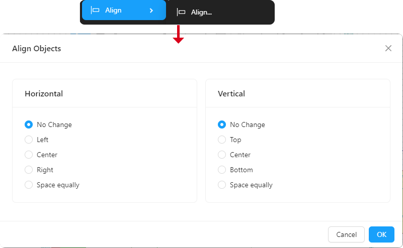
Figure 4-9
Lock and unlock, and lock and unlock the selected elements for their location and related attributes. The locked element will not be able to change its relevant properties, and can only be changed after unlocking the operation. When the position moves, the "confirm" window (Figure4-10) will pop up, indicating whether to continue to move the locked element。
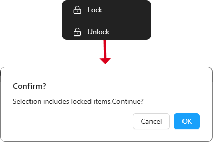
Figure 4-10
Find and replace relevant elements in the SCH file,The content you can search for and replace includes reference designators, text, global labels, port labels, net labels, or all of the above (Shortcut key Ctrl + F)。
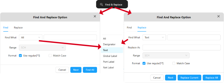
Figure 4-11
Offset the position coordinates of the selected elements. There are two methods of offsetting, as shown in Figure 4-12。
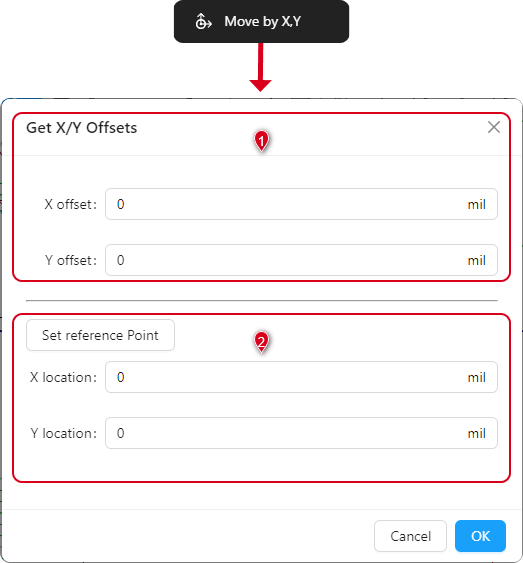
Figure 4-12
Method 1: Use the element's own coordinates as the reference point, enter the offset values for the X and Y axes, and perform the offset operation based on its own coordinate position
Method 2: Manually set the reference point with the mouse cursor, input the offset values for the X and Y axes, and perform the offset operation based on the coordinates of the set reference point。
Note: The top-left corner of the canvas is the coordinate origin (X=0, Y=0)。

Figure 4-13 shows the coordinate position of R1 before offsetting
Figure 4-14 shows R1 being offset by method 1 (using its own coordinates as the reference point), with both the X and Y axes offset by 2mm。
Figure 4-15 shows R1 being offset by method 2 (using pin 2 of R2 as the reference point), with both the X and Y axes offset by 2mm。
Sequentially reset the reference designators of components on the canvas in a 'Z' pattern, from left to right, from top to bottom.

Figure 4-16 shows the components before reference designator reset, andFigure 4-17 shows the components after the reference designator has been reset.
After selecting the trace break function, use the cursor to box-select the region where the trace needs to be interrupted to perform the break operation (as illustrated in Figure 4-18)。

Figure 4-18
 6.3.3 View Menu
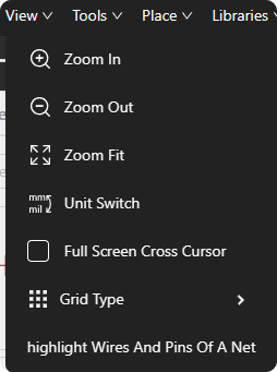
Figure 4-19
Zoom in on a specific area within the view to examine design details more closely. This is particularly useful for looking at small components or details in complex circuits, helping design engineers to adjust and analyze the circuitry more precisely.(Shortcut key Page Up)
Zoom out of a specific area within the view to see the overall design in a broader perspective. This helps design engineers to quickly navigate between different levels of the design, locating key modules or connections。(Shortcut key Page Down)
Zoom Fit:The fit-to-screen feature allows the entire design to be scaled to fit within the current screen, ensuring that the entire design is visible within one screen. This is very useful for quickly reviewing the overall layout and connections of the design without needing to manually adjust the zoom level。
Unit Switch:Switch between units of mil (thousandths of an inch) and mm (millimeters)。(Shortcut key Q)
Full Screen Cross Cursor:After selecting this option, a crosshair cursor will be displayed over the entire design interface, allowing for more accurate measurement and positioning of components, traces, or other design elements

Figure 4-20
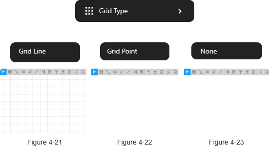
Grid Type: Used as an alignment reference for component symbols, signal traces, and other elements on the design interface,primarily available in three styles: Grid Line, Grid Point, and None。
After selecting this feature, the chosen net and its pins will be highlighted. Figure 4-24 shows the GND net selected in the SCH, highlighting the GND net traces and the pins of devices it connects to throughout the design。
Figure 4-24
 6.3.4 Tools Menu

Figure 4-25
ERC:Electrical Rule Checking
Used to verify whether the circuit design complies with electrical rules. ERC (Electrical Rule Check) is an automated checking tool that can identify potential electrical issues at various stages of the design process, helping design engineers to discover and resolve problems early, thus improving the quality and reliability of the circuit design.
After running the ERC check, a results window will appear (as shown in Figure 4-26), with the left side of the window reporting the types and quantities of errors, and the right side providing information about the constraint names (content of the error objects), current page (the page where the error item is located), and the ERC error location (the coordinate position in the schematic)。
The types of errors checked by the ERC function include the following eight categories:
1、Check single node nets: Ensure there are no single-pin nets, meaning that all nets should connect at least two components to avoid floating signals or unused pins。
2、Detect unconnected network labels: Search for net labels that are not connected to any components to ensure that all signals are correctly connected to the components in the circuit。
3、Check for duplicate tags: Ensure that the same reference designators are not used more than once in the circuit design, to avoid confusion and incorrect connections。
4、Check unconnected pins: Search for pins that are not connected to other components, to ensure that all component pins are correctly connected to other elements within the circuit。
5、Check device with zero pins: Ensure that all devices have pins to prevent the occurrence of devices without pins。
6、Check symbol and Footprint pin consistency: Ensure that the pins defined in the symbols and footprints are consistent to avoid incorrect connections。
7、Check power ground short: Search for shorts between power and ground to ensure the correctness of power distribution and to prevent power-ground shorts。
8、Check for missing Footprints:Ensure that each component has a corresponding footprint defined to guarantee that the PCB layout and the component packaging match correctly。

Figure 4-26
Update PCB:After completing the circuit diagram drawing design and loading all the components Footprint, the content in the schematic editor can be updated to the PCB editor. After selecting this function, the encapsulation check window will pop up, including serial number, bit number, encapsulation and report. Figure 4-27 shows the error between the schematic symbol and PCB encapsulation pin; Figure 4-28 shows the repetition of the schematic symbol bit number; Figure 4-29 shows the components without associated packaging。
It is recommended to modify the relevant errors according to the report content until you click "Update PCB”。
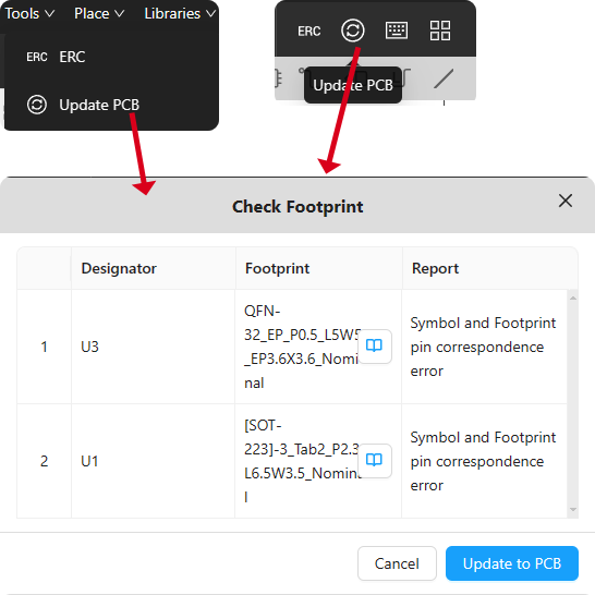
Figure 4-27
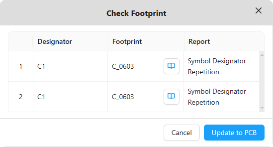
Figure 4-28
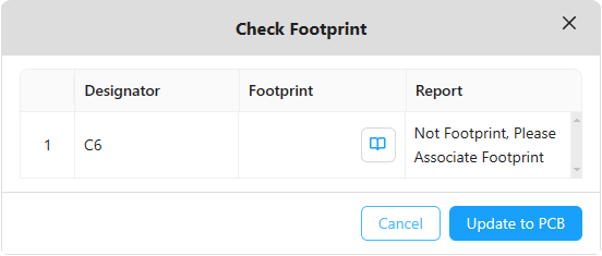
Figure 4-29
Click on the icon in the 'Footprint Check' window,Popup the Footprint Library window (Figure 4-30)。
Footprint library types are categorized as two types,The public footprint library contains three main categories: 'Common Components,' 'Generic Footprints,' and 'Connectors.' Select the appropriate footprint based on the schematic component symbol and the physical component. If a suitable component footprint is not found in the public library, it can also be drawn and designed according to the Footprint size information in the component manual (detailed operations are explained in the section on Footprint design). Custom-designed footprints will be saved under the category of footprint library types。
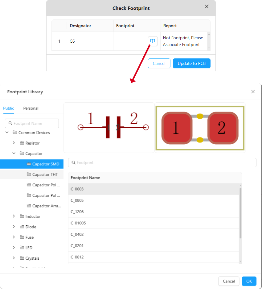
Figure 4-30
After confirming the option to update to PCB,The SCH editing page will switch to the PCB editing page, and the 'Update PCB Design' window will appear. After checking the components that need to be updated to PCB, click the 'Update' option。

Figure 4-31
After confirming the update, the updated component footprints will be displayed in the top-left corner of the PCB editing page, where you can then adjust the positioning of the component footprints and proceed with the PCB routing design。
Figure 4-32
Array Copy:Array functionality is used to easily replicate and align elements, signals or other design elements to improve the efficiency and accuracy of design. Array functionality is usually used to place a large number of similar or repetitive elements on a circuit board。
Note: You need to select the elements that require the array first, and then click on the array function。
After clicking on the array feature, the 'Array Object' parameter setting window will pop up. The parameters available for setting include:
Rows: Specifies the number of rows in the array, that is, the vertical quantity of the elements to be copied;
Row Spacing: Defines the distance between adjacent rows, which is the vertical distance between two rows;
Columns: Specifies the number of columns in the array, or the horizontal number of replicated elements;
Column spacing: Defines the spacing between adjacent columns, the horizontal distance between two columns;
Direction: Specifies the direction of the array, with options to select Horizontal priority (Horizontal first) or Vertical priority (Vertical first);
Primary:Allows the user to specify the increment value for the text of each element in the array (such as reference designators in SCH and PCB interfaces, pin numbers in symbol interfaces, and pad numbers in footprint interfaces), so that increments can be applied between rows or columns;
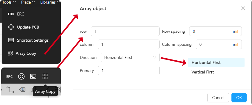
Figure 4-33
Shortcut Settings:Click the "Shortcut Settings" option to display the "Shortcut Settings" window (Figure 4-34). If you need to change the shortcut key setting, after moving the cursor to the corresponding cursor line, the keyboard can directly press the key used to be changed, and then complete the shortcut key to change the setting。

Figure 4-34
Table 4-1 is the system default settings for all shortcut key commands in PCBX。
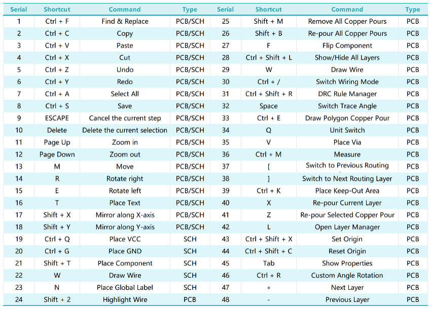
Table 4-1
Footprint Manager:The Footprint Manager function is used to manage the Footprint information for the electronic components. Includes the physical dimensions, pin definition, 3D models, layout and other information。
Click the "Packaging Manager" function to display the "Symbol attribute Table" window (Figure 4-35). The part on the left side of the window is the list of devices, which includes the bit number, value, description, device type, packaging, drawing, material number, and manufacturer. Click the corresponding content to order the device in ascending / descending order。
Select the most left check box of the device list in the window to view and edit the Footprint of the corresponding device, and more of the Footprint devices of the same type can be selected for viewing and editing。
After checking the corresponding components, you can view or edit the Footprint in the right half of the "Symbol attribute Table" window. The upper right part is the view and selection of the component Footprint type, and you can add or delete the Footprint。
Click after clicking on the option, the 'Footprint Library' window will pop up (as shown in Figure 4-30). In the library, you can select the appropriate footprint to add。
In the 'Symbol Attribute Table' window, the bottom right section provides a preview of the component effects, from left to right, showing the schematic symbol, PCB footprint symbol, and the PCB footprint 3D rendering。
In the 'Symbol Attribute Table' window, the lower left section shows the number of component symbols in the drawing and the number of component symbols that are editable。
 After completing the footprint editing, click to finalize the changes。
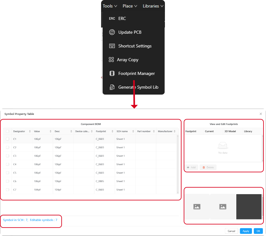
Figure 4-35
Generate Symbol Lib:This feature is designed to extract symbols from the schematic of the current project and create a symbol library, which can then be further edited in the Symbol Editor. The symbol library includes schematic symbols of components, which can be utilized in other schematic designs。
After clicking the 'Generate Symbol Library' option, a 'Generate Symbol Library' window will pop up (as shown in Figure 4-36),First, edit the name of the symbol library; the name must not exceed 200 characters。After entering the library name, click 'OK' or click 'Generate and Enter。

Figure 4-36
Component Symbol Selection:After clicking 'OK,' you can see the newly created symbol library in the 'Component Symbol Selection Area' on the left side of the editor interface (as shown in Figure 4-37).
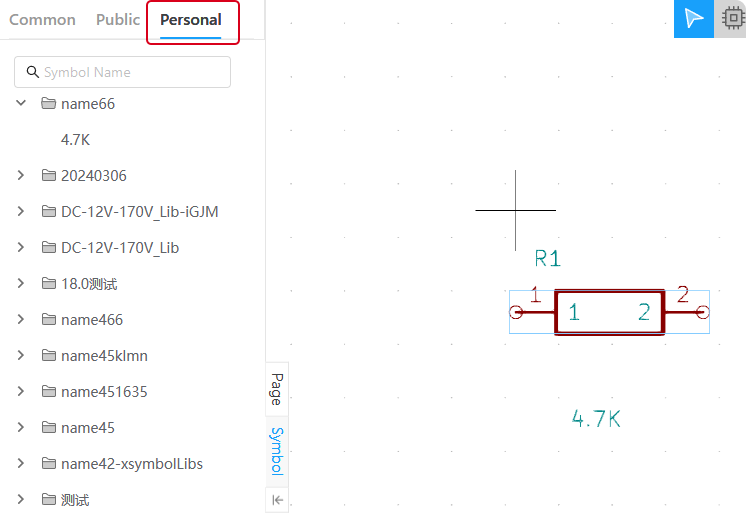
Figure 4-37
After clicking 'Generate and Enter,' the page will automatically switch to the Symbol Editor interface (as shown in Figure 4-38). Select the corresponding component symbol for secondary editing (as shown in Figure 4-39)。
Figure 4-38
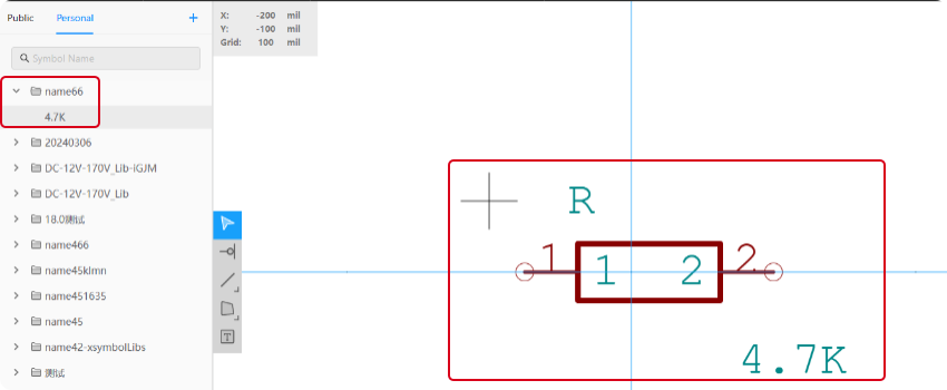
Figure 4-39
 4.3.5 Place Menu
Used for placing (adding) components, graphics, text, and more into the schematic。
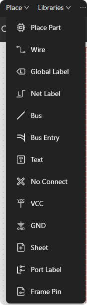
Figure 4-40
Place Part:Double-click to place electronic components (such as resistors, capacitors, etc.) or click 'Place' to add them to the schematic, followed by proper positioning。(Shortcut key Shift + T)
After clicking the 'Place Part' function, the 'Part Search' window will pop up (as shown in Figure 4-41)
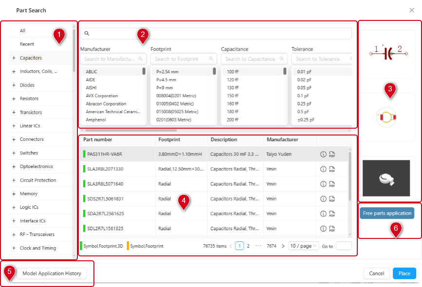
Figure 4-41
“Part Search”
Window section ① : Select the type of component ;
Window section ② : Filter and search for components,For example, ceramic capacitors can be based on the Manufacturer of the components、Footprint、Capacitance、Tolerance、Voltage Rating、Dielectric、Height - Seated (Max)、Thickness and Packaging Filter and search based on conditions;
Window section ③ : For the component symbol preview, from top to bottom, respectively Symbol、Footprint、3D Model。
Window section ④ : Select the specific model number for the component type, the display content is Part number(Component Part Number)、Footprint(Footprint Type)、Description(Component Parameters)、Manufacturer;Within the color block to the left of the Part number Green indicates that the component symbol includes a schematic Symbol、 Footprint and 3D Model,while orange indicates that the component Symbol includes a schematic Symbol and Footprint。After clicking the symbol to the right in the component selection, a detailed component parameters window will pop up,View related detailed parameters。
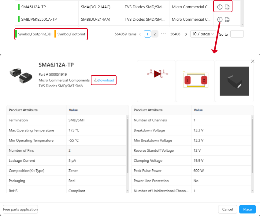
Figure 4-42
Click on the 'Detailed Component Parameters' window Or in the 'Component Placement' window section ④ You can download the device manual。
“Part Search”Section ⑤ in the window is for component model application,After clicking the 'Free parts application' option, a 'Free parts application' window will pop up (see Figure 4-43),After filling in the Part number, Manufacturer, Missing (the application can choose schematic Symbols, Footprint, and 3D models), and more information (other attributes of the component or a brief description), confirm the application。

Figure 4-43
“Part Search”Section ⑥ in the window is for viewing the history information of component model applications,After clicking the 'Model Application History' option, a 'Model Application History' window will pop up ( Figure 4-44),The content viewed in the model application history includes the Part number, Project name, Manufacturer, Model, State, and Date. It is possible to query based on Part number/Project name, State, and Date range. The status options include all, pending, processing, and updated。
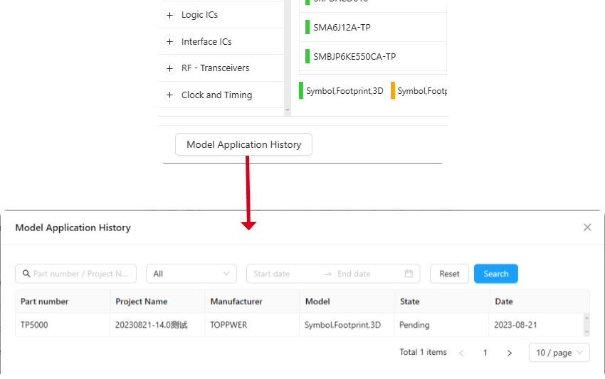
Figure 4-44
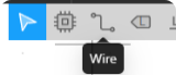
Wire:Connect the pins between components to form electrical connections。 After selecting this function, the cursor in the editing interface will change to.(Shortcut key W)

Place global labels (Global Labels), which can be used to identify global signals in the circuit。These signals are typically shared throughout the entire design, such as clock signals, reset signals, or other control signals that are used throughout the entire design。Global labels help to simplify the understanding, management, and maintenance of a circuit。(Shortcut key N)
After clicking the 'Global Label' function option, a 'Place Global Net Label' window will pop up (Figure4-45)。
Enter the name of the global net label, select the electrical type and shape size, then click 'OK' to place the global net label. The electrical type by default is set to input, with options for input, output, passive, and bidirectional; the default shape size is 40, with a selectable range of 26-46 (with an increment of 2)。

Figure 4-45
Place net label(Net Labels),Net labels are used to identify electrical connections or signals in circuit designs。Net labels allow designers to provide a name for specific electrical connections in a circuit, enabling them to be uniquely identified and referenced throughout the design。Using net labels can simplify the wiring of a circuit, as it is not necessary to draw the connecting wires directly to each connection point。The same net label can only be interconnected within a single schematic diagram。
After clicking the 'Net Label' function option, a 'Place Net Label' window will pop up (Figure 4-46)。
Enter the name of the net label, choose the size, and click 'OK' to place the net label. The default size is 40, with the selectable range from 26 to 46 (in increments of 2)。
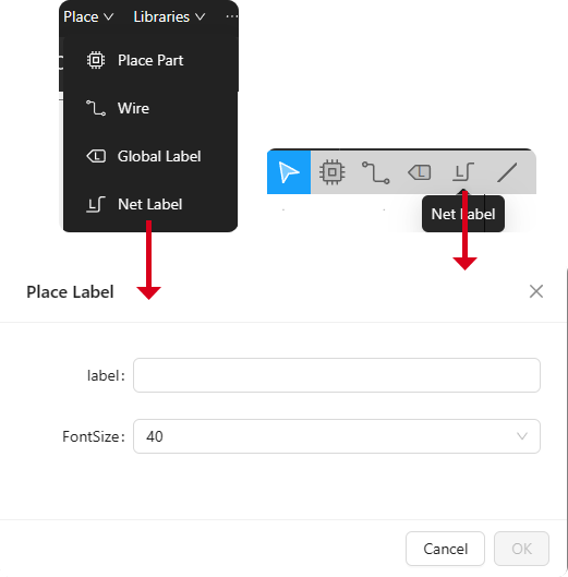
Figure 4-46
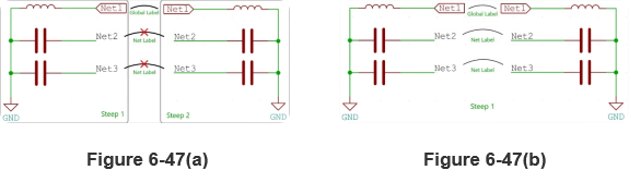
Comparison of the use of Global labels and Net labels:
Global label:Global labels with the same name across multiple schematic sheets can be interconnected。
Net label:The same net label can only interconnect within a single schematic diagram。
As shown in Figure 4-47, global labels can interconnect between multiple schematic sheets, whereas net labels can only interconnect within the same circuit schematic。
Net labels from different pages can be interconnected across pages by placing global labels with the same network name on the same page。
Place Bus Placement:They are used to create and manage bus structures in circuit design. A bus is a way to organize multiple signals together, allowing designers to handle and connect a large number of signals more efficiently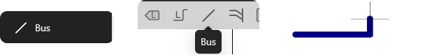
Place Bus Entryfunction is typically related to schematic editing and the creation and management of buses. A bus entry is used to introduce a bus into the design and connect it with other components。
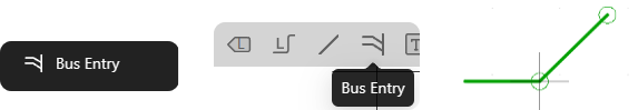
Figure 4-48 is an example of the use of buses and bus entries。
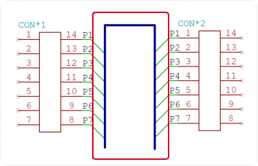
Figure 4-48
Place Text:The function of adding text labels in the schematic, allowing designers to add necessary notes, explanations, or other textual information to the schematic for a clearer expression of the design's intent and explanation. After clicking the 'Text' function option, a 'Place Text' window will pop up (see Figure 4-49)。(Shortcut key T)
Enter the text content (use the shortcut key Shift + Enter to line break), select the shape size and origin position, and then click 'OK' to place the text. The default shape size is 40, with a selectable range of 26-46 (with a selection precision of 2); the text origin position (used as a reference position for alignment) can be set to one of nine positions: top, bottom, left, right, top-left, top-right, bottom-left, bottom-right, or center。

Figure 4-49
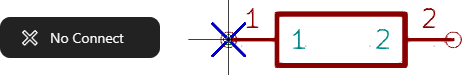
Place No Connect:Used to indicate that certain component pins or nodes are not connected to other parts of the circuit. Some pins may be unused, not required to be connected, or are used only for internal purposes and not connected to the external circuit。In these cases, it is necessary to mark the component or pin as "No Connect," indicating that they have no actual connections in the circuit, and thus will not trigger errors for "Check unconnected pins" during the Electrical Rules Check (ERC)。
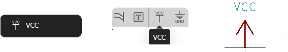
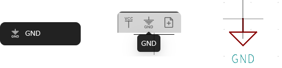
Place VCC :(Power supply voltage),adds a marker symbol in the schematic diagram to indicate a power supply connection. This is used to identify the locations where specific component pins are connected to the power supply voltage VCC。 (shortcut key Ctrl + Q)
Place GND (Ground wire),adds a marker symbol in the schematic diagram to indicate a ground wire connection. This is used to identify the locations where specific component pins are connected to the ground wire。 (shortcut key Ctrl + G)
Add Sheet:Used to create and manage different levels in hierarchical designs. Hierarchical sheets are diagrams representing different modules or subsystems in a circuit design. The use of hierarchical sheets helps designers to better organize and manage complex circuit designs by dividing them into modules that are easier to understand and maintain。
After clicking the 'Hierarchical Sheet' function option, an 'Add Sheet' window will pop up (Figure 4-50)。
Enter the sheet name and choose the reference sheet, then click 'OK' to add the hierarchical sheet。

Figure 4-50
Place Port Label。In hierarchical design, sheet port labels are used to connect circuits across different levels。 Mainly used to identify the pins of components, especially those that connect with other modules or systems。Typically, port labels are used to represent the function of pins such as input, output, power, and ground。
After clicking the 'Port Label' function option, a 'Place Port Label' window will pop up ( Figure 4-51)。
Enter the port label name, select the electrical type and shape size, then click 'OK' to place the port label. The electrical type is default set to input, with selectable options including input, output, passive, and bidirectional; the default shape size is 40, with a range of 26-46 available (in increments of 2)。
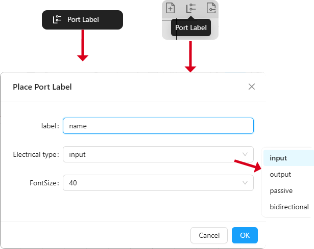
Figure 4-51
Place Frame Pin,Used to create and manage sheet ports in hierarchical designs, these ports allow for connections within different levels of the design。
Sheet、Port Label andFrame Pin Usage Example。
 Add Sheet: As shown in Figure 4-52, click on the icon to the left of the Sheet1 schematic in the project SCH,After opening the checkbox, selec Add SCH,Upon completion of the addition, the newly added Sheet2 schematic will be displayed within Sheet1。After adding a new page, then select the 'Add Sheet' function。At this point, the interface will pop up with the 'Add Sheet' window as shown in Figure 6-49. After entering the sheet name Sheet2 and selecting Sheet2 for the reference, click OK。
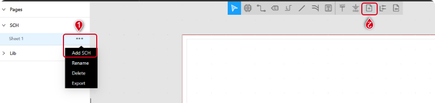
Figure 4-52
At this time, Sheet2 in the left page section will become a sub-level of Sheet1, as shown in Figure 4-53。
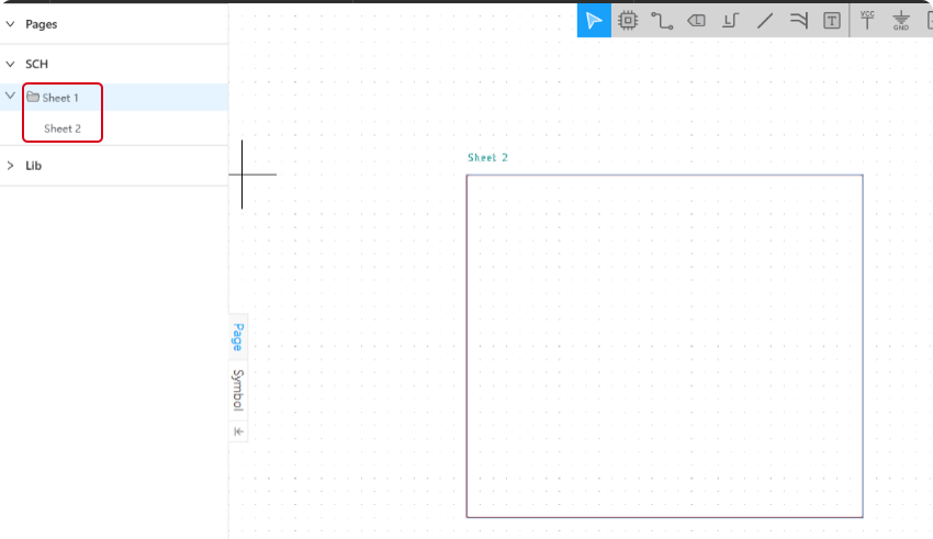
Figure 4-53
Place Port Label:After completing the addition of the hierarchical sheet, start drawing the sub-circuit diagram (Sheet2) and placing the port net labels. As shown in Figure 4-54, a resistor R1 and a port label Net1 are placed in the Sheet2 schematic, and Net1 is connected to pin 2 of R1。

Figure 4-54
Place Frame Pin:As shown in Figure4-55, after placing the port label, return to the Sheet1 schematic page. In the Sheet1 schematic, place resistor R2 and place the Sheet Port Net Net1 within Sheet2 on Sheet1. Then connect Net1 to pin 1 of R2
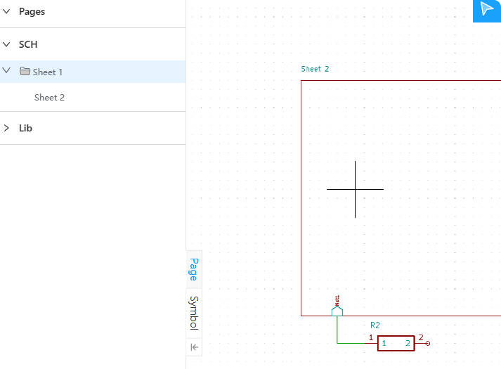
Figure 4-55
As shown in Figure 4-56, after completing the above operations, update the schematic to the PCB, and you can see that pin 1 of R2 and pin 2 of R1 belong to the same network (Net1) in the PCB editor page. This completes the use of the hierarchical sheet port net label。

Figure 4-56
6.4 SCH Design - Toolbar

Figure 4-57
1、Save
2、Undo
3、Redo
4、Align
5、Lock
6、Unlock
7、Find & Replace
8、Move by X,Y
9、Designator Reset
10、Refresh: Refresh the editing interface。
11、Zoom In
12、Zoom Out
13、Zoom Fit
14、Unit Switch
15、Grid Setting: Set the cursor (element) moving increment
16、Grid Type
17、ERC
18、Update PCB
19、Shortcut Settings
20、Array Copy
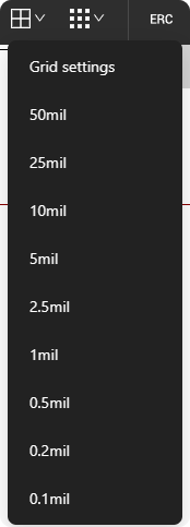
Figure 4-58
For commands that have not been detailed above, please switch to Section 4.3 SCH Design - Menu Bar for detailed explanations。
6.5 Symbol and Page Selection
As shown in Figure 4-59, on the right side of the 'Component Symbol and Page Selection Area', you can switch between the project and symbol menus. Figure 4-60 is the component symbol selection area, with the component Symbol source selection at the top of the area, where you can choose from Common used symbols, Public, Personal。

Figure 4-59

Figure 4-60
Figure 4-61 is the Pages drawing selection area。

Figure 4-61
6.6 Cursor Coordinate Display
Figure 4-62 shows cursor coordinate position information, where the grid points represent the set grid spacing。

Figure 4-62
6.7 SCH Toolbar
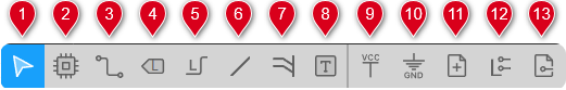
Figure 4-63
1、Select
2、Place Part
3、Place Wire
4、Place Global Label
5、Place Net Label
6、Place Bus
7、Bus Entry
8、Place Text
9、Place VCC
10、Place GNG
11、Add Sheet
12、Place Port Labe
13、Place Frame Pin
6.8 Schematic Design Section
As shown in Figure 4-64, the area enclosed by the box is the schematic design area。
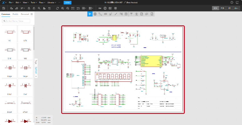
Figure 4-64
In the bottom right corner of the schematic design area, there is the title block of the circuit diagram (Figure 4-65). After double-clicking in this area with the cursor, a Document Properties window will pop up on the right side of the page, where you can edit the document canvas parameters:
Switch(mm / mil);
Grid Type(Grid Line、Grid Point、None);
Standard Sheet Sizes(A1、A2、A3、A4),Sheet Orientation(Horizontal / Vertical);
Custom Sheet Sizes(Manually enter the sheet width and height);
Title Bar(Optionally show or hide);
Page margins: Vertical distance and Horizontal distance;
Show Zones(Optionally show or hide;
Version;
Drawed。
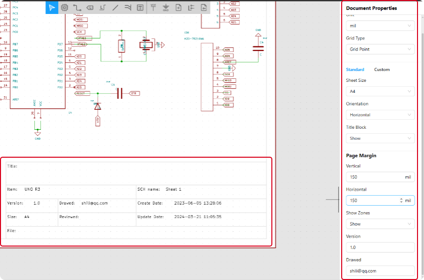
Figure 4-65
Similarly, by double-clicking on the corresponding element symbol in the schematic design area, a property parameter window for that element will pop up on the right side of the page. The following figure shows the property parameter window for the related elements。
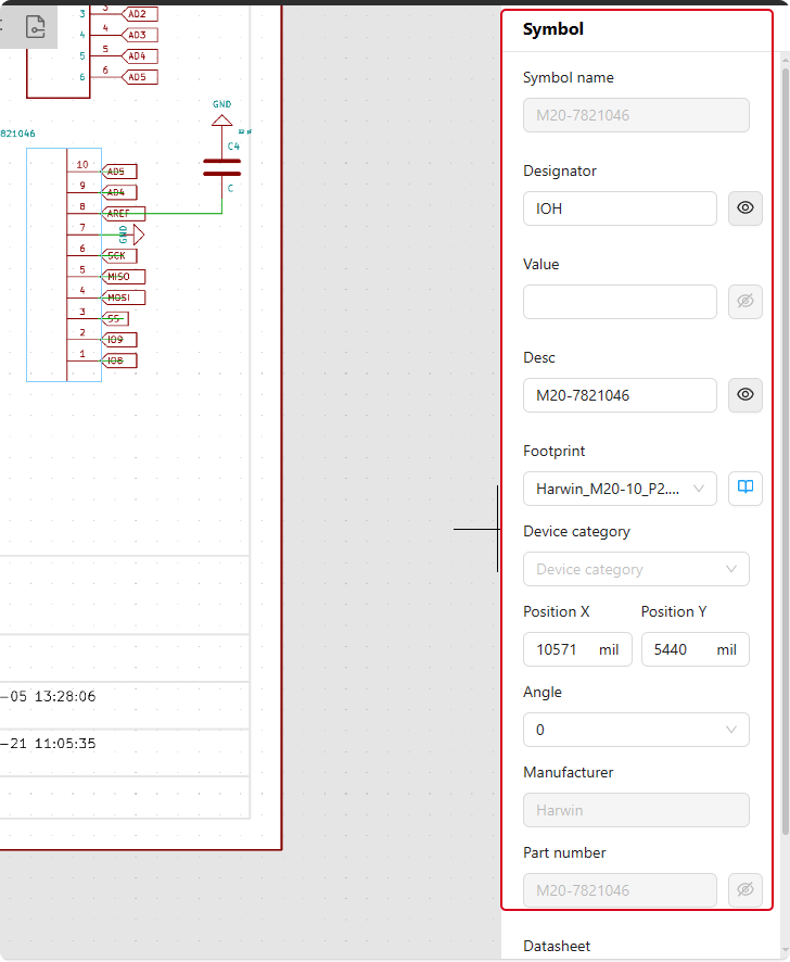
Figure 4-66(Symbol attribute)

Figure 4-67(Route)
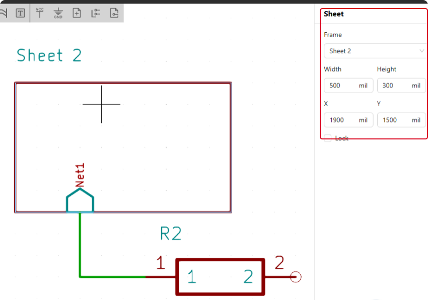
Figure 4-68(sheet)
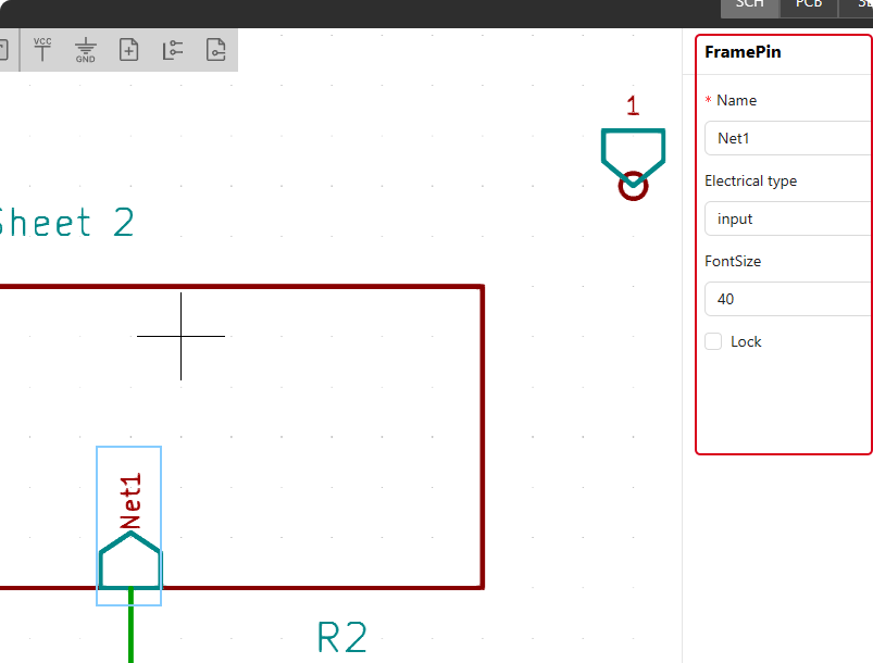
Figure 4-69(FramePin)
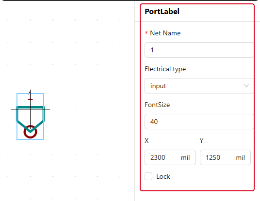
Figure 4-70(PortLabel)
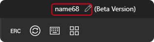
6.9 Project Name Editing
You can type and modify the project name in the project file name editing area。
6.10 Editor Switching
In the main editing area of the interface, you can switch between different editors, including the Schematic (SCH) editing interface, PCB editing interface, 3D preview interface, and the Library editor (Lib). The Library editor allows further selection among the Symbol Editor, Footprint Editor, Padstack Editor, and Part Editor。

6.11 Guide and Share
 Click on the guidance icon A Getting Started Guide window will pop up (Figure 4-71)。
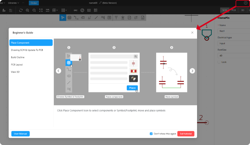
Figure 4-71
Click on the share icon the system will automatically generate a share link (Figure 4-72). Click 'Copy' next to the link to copy the share link to the clipboard for pasting and sharing。

Figure 4-72