
6、 Libraries
Libraries are tools used to create, edit, and manage symbol libraries and footprint libraries for components. These libraries are used to store information about the symbols and footprints of components, making them available for use in schematic diagrams and PCB designs. You can access the Symbol Editor, Footprint Editor, Padstack Editor, and Part Editor either from the Library Editors in the menu bar at the top of the editing page (Figure 6-1(a)), or from the toolbar on the right side just below the top of the editing page (Figure 6-1(b))。

6.1 Symbol Editor
The tool used to create and edit schematic symbols for components. This editor allows designers to define the appearance, pin connections, and other relevant information for components. Figure 6-2 shows the main interface of the Symbol Editor。
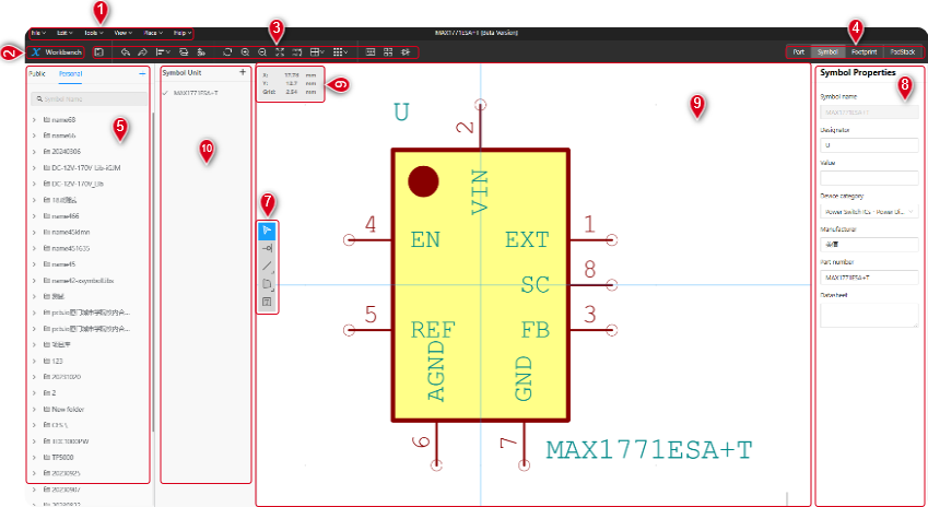
Figure 6-2
1、Menu Bar
2、Workbench
3、Toolbar
4、Editor Switching
5、Symbol Library
6、Cursor Coordinate Position
7、Symbol Toolbar
8、Symbol Properties
9、Symbol Drawing
10、 Symbol Unit
6.1.1 Menu Bar
6.1.1.1 File Menu
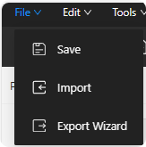
Figure 6-3
Save:Refer to the same function in the SCH Edito。(Shortcut key Ctrl + S)
Import: After selecting import, the page will pop up the "Import Symbol Library" window (as shown in Figure 6-4). The file formats supported are .kicad_sym, .xsymlib, .lib, and .lbr。

Figure 6-4
Export Wizard:After selecting the "Export Wizard" option, the page will pop up the "Export Wizard" window (as shown in Figure 6-5). In the window, choose the symbol library folder that needs to be exported from the list.。
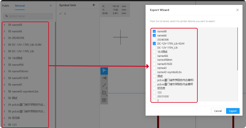
Figure 6-5
6.1.1.2 Edit Menu
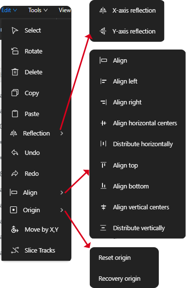
Select(Refer to in SCH)
Rotate(Refer to in SCH )
Delete(Refer to in SCH)
Copy(Refer to in SCH )
Paste(Refer to in SCH )
Reflection(Refer to in SCH )
Undo(Refer to in SCH )
Redo(Refer to in SCH )
Align(Refer to in SCH )
Origin(Refer to in SCH )
Move by X,Y(Refer to in SCH )
Slice Tracks:Different from the Slice Tracks feature in SCH and PCB layouts, which uses a box selection method to break tracks, the Break Wire function in the symbol editor uses a line selection method。
Select the "Slice Tracks" tool, click on the starting position, drag the mouse and click on the ending position; the line segment picked by the line selection will then be severed. Figure6-7 shows the comparison before and after using the Break Wire feature。

Figure 6-7
6.1.1.3 Tools Menu
Symbol wizard tool:The feature assists designers in quickly creating schematic symbols that conform to standards. It provides an interactive wizard interface (Figure 8-8) that guides users through the symbol creation process。
After clicking on "Symbol Wizard Tool" in the Tools menu bar, the "Symbol Wizard" window will pop up (Figure 6-8). Designers can set the relevant attribute parameters for creating a new symbol based on the contents of the window. Parameters that can be set include Number of Pins, Layout Pin Style, Name, Pin Number, Electrical Type, and Side, among others。
(1)Number of Pins:You can specify the number of pins for the component. The Symbol Wizard will automatically generate the corresponding number of pins based on this parameter。
(2)Layout Pin Style:You can choose the arrangement of the pins, with available styles including U-shaped(Dual 1), Z-shaped(Dual 2), N-shaped(Dual 3), single row, and custom. You can select the pin arrangement style that is suitable for different components。
(3)Name:Specify a name for each pin. These names are used to identify the function or connection of the pins。
(4)Pin number:Corresponds one-to-one with the actual Footprint pin numbers and must not be duplicated.。
(5)Electrical Type:You can specify the electrical type for each pin, with options including Input, I/O, Output, Open-collector, Passive, Open emitter, Power-in, or Power-out. This helps ensure the correctness of electrical connections。
(6)Side:You can specify the orientation of each pin on the symbol, with options including Up, Down, Left, or Right. On the right side of the "Symbol" wizard window, there is a preview image of the symbol with the wizard settings。
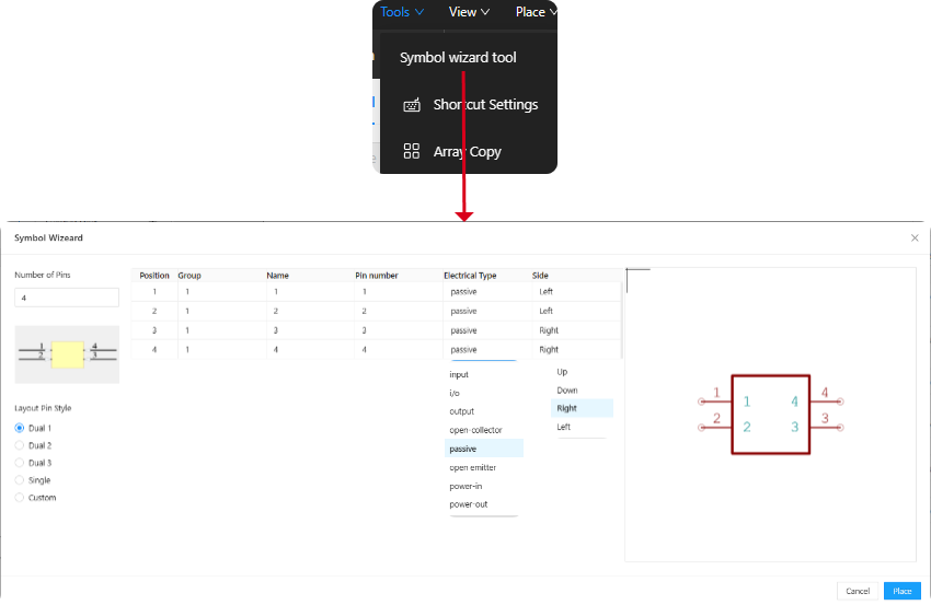
Figure 6-8
Shortcut Settings:(Refer to in SCH )
Array Copy:(Refer to in SCH )
6.1.1.4 View Menu
Zoom in:(Refer to in SCH )
Zoom out:(Refer to in SCH )
Zoom fit:(Refer to in SCH )
Grid Settings:(Refer to in PCB )
Grid Type:(Refer to in PCB )
Unit switch:(Refer to in PCB)
6.1.1.5 Place Menu
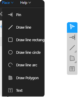
Figure 6-10
Place Pin:Used to define the electrical connections of a component. Select the pin tool, click on the position where the pin is to be placed; adjust the attributes of the pin, such as direction, electrical type, number, name, length, position, part selection, etc。
Draw line:Select the line segment tool, click on the starting position, drag the mouse and click on the ending position; adjust the attributes of the line segment, such as line width, position, etc。
Draw line rectangle:Select the rectangle tool, click on one corner of the rectangle, drag the mouse and click on the opposite corner; adjust the properties of the rectangle, such as line width, width, height, position, and fill style, etc. (Fill style options include none, fill style 1, and fill style 2) 。
Draw line circle:Select the circle tool, click on the center of the circle, drag the mouse and click on the boundary of the circle; adjust the properties of the circle, such as line width, position, radius, and fill style (three fill styles are available: no style, fill style 1, and fill style 2)。
Draw line arc:Select the arc tool, click on the center, starting point, and ending point of the arc; adjust the properties of the arc, such as line width, starting angle, ending angle, position, radius, and fill style (three fill styles are available: no style, fill style 1, and fill style 2)。
Draw Polygon:Select the polygon tool and click on each vertex of the polygon in sequence. Adjust the properties of the polygon, such as line width, position, and fill style (three fill styles are available: no style, fill style 1, and fill style 2)。
Place Text:To annotate symbols on a circuit diagram or other design elements, select the text tool, click on the location where you want to place the text, and a "Text Edit" window will pop up. In the "Text Edit" window, select the text size (with a selectable range from 26 to 46), enter the text content, and then click apply。
6.1.2 Workbench
Return to the workbench:After clicking this icon, the page will return to the workbench。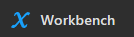
6.1.3 Symbol Design - Toolbar

Figure 6-12
1、Save
2、Undo
3、Redo
4、Align
5、Show/Hide Left Sidebar:As shown in Figure 6-13, this is used to show or hide the symbol component selection sidebar on the left side of the symbol editing page; clicking the "+" icon will allow the creation of multi-part symbols。
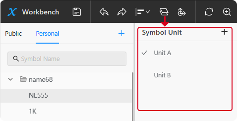
Figure 6-13
6、Move by X,Y
7、Refresh: Refresh the editing interface。
8、Zoom in
9、Zoom out
10、Zoom fit
11、Unit switch
12、Grid Settings
13、Grid Type
14、Shortcut Settings
15、Array Copy
16、Create New Symbol: After clicking this icon, a "New" window will pop up (as shown in Figure6-14), where you can enter the name of the component symbol, select the device type, choose the address of a Personal symbol folder, and then click OK。
Note:Before adding a new symbol, there must be at least one folder in the Personal symbol folder directory. If there is no folder within the component symbol Personal library, a new one must be created (as shown in Figure 6-15)。
1、In the "Symbol Library" window on the left side of the page, select "Personal.";
2、Click the "+" icon at the top right corner of the window;
3、Enter the name of the folder in the newly popped-up rectangular box and
press Enter to confirm.
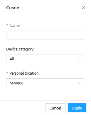
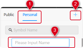
Figure 6-14 Figure 6-15
6.1.4 Switch the editing interface
Switch the editing interface:Switch between the Symbol editor,Footprint editor, PadStack editor, and Part editor pages。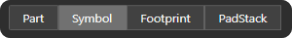
6.1.5 Symbol Library
The Symbol Library window is divided into two parts: "Public" and "Personal" (as shown in Figure 6-16). In the "Personal" window, there are two main categories: connectors and commonly used components. The "Personal" window contains Personal library folders and component symbols created by the user for personal use。
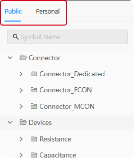
Figure 6-16
6.1.6 Cursor Coordinate Position
Display the current cursor position and grid unit information on the canvas (as shown in Figure 4-61)。
6.1.7Symbol Toolbar
Select
Place Pin
Draw line
Draw line arc
Draw line circle
Draw line rectangle
Draw Polygon
Place Text
6.1.8 Symbol Properties
The interface is used to view and edit the attributes of component symbols. The window editing information includes symbol name, pin number, value, device type, manufacturer, part number, and datasheet。
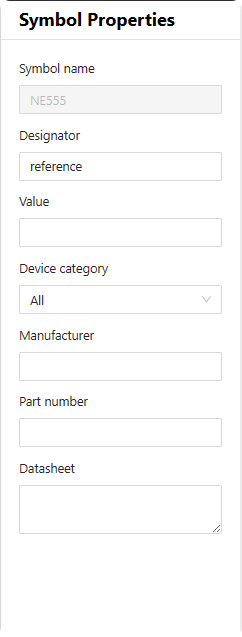
Figure 6-17
6.1.9 Symbol Design Section
The main work area for users to design and edit component symbols. Users can create, modify, and adjust the circuit diagram symbols of components in the canvas area。
6.2 Footprint Editor
A tool for creating and editing the enclosures or libraries of electronic components. The Footprint describes the physical appearance, pin layout, dimensions, materials, and other information of the component, so that it can be laid out and routed in PCB design. Figure 8-18 is the main interface of the Footprint editor。
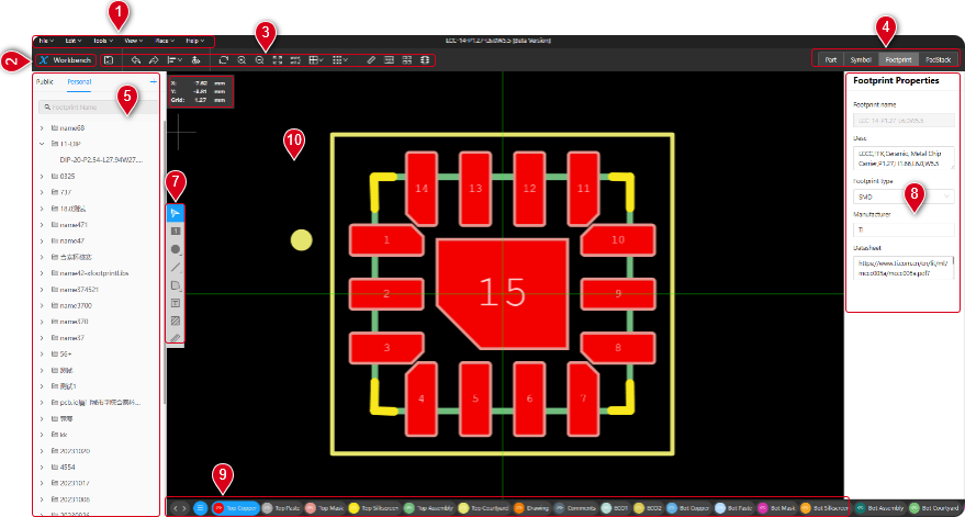
Figure 6-18
1、File Menu
2、Workbench
3、Footprint Design - Toolbar
4、Switch the editing interface
5、Footprint Library
6、Cursor Coordinate Position
7、Symbol Toolbar
8、Footprint Properties
9、Footprint Layer Selection
10、Footprint Design Section
6.2.1 Menu Bar
6.2.1.1 File Menu
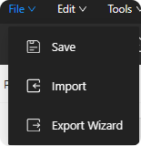
Figure 6-19
Save: saves the changes made in the current Footprint editing session。(Shortcut key Ctrl + S)
Import: Translation: After selecting to import, a "Import Footprint Library" window will appear on the page (as shown in Figure 6-4), with file formats being .Zip, .xfootlib, and .lbr。
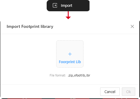
Figure 6-20
Export Wizard:After selecting the "Export Wizard" option, the "Export Wizard" window will pop up (as shown in Figure 6-21). In the window, select the footprint library folder you wish to export from the list。

Figure 6-21
6.2.1.2 Edit Menu
Select(Reference PCB)
Rotate(Reference SCH)
Delete(Reference SCH)
Copy(Reference SCH)
Paste(Reference SCH)
Reflection(Reference SCH)
Undo(Reference SCH)
Redo(Reference SCH)
Align(Reference SCH)
Origin(Reference PCB)
Move by X,Y(Reference Symbol Editor)
Slice Tracks(Reference Symbol Editor )
6.2.1.3 Tools Menu
Measurement(Reference PCB)
Shortcut Settings(Reference SCH)
Array Copy(Reference SCH)
6.2.1.4 View Menu
Zoom in(Reference SCH)
Zoom out(Reference SCH)
Zoom fit(Reference SCH)
Unit switch(Reference PCB)
Grid Settings(Reference PCB)
Grid Type(Reference PCB)
6.2.1.5 Place Menu
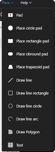
Figure 6-25
Pad: Select the pad tool, and a "Pad" window will pop up (as shown in Figure 6-26). Designers can choose an appropriate existing pad template from the public pad library to place or select a self-drawn pad from the Personal library for placement.。

Figure 6-26
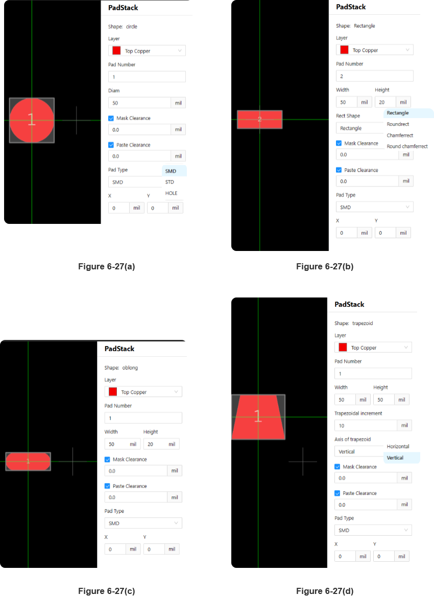
Place circle pad:Select the circular pad tool, adjust the properties of the circular pad, such as stack, pad number, diameter, solder mask clearance, pad type and position, etc. (as shown in Figure 6-27(a))。
Place rectangle pad:Select the rectangular pad tool, adjust the properties of the rectangular pad, such as stack, pad number, width and height, rectangle type, solder mask clearance, pad type, and position, etc. (as shown in Figure 6-27(b))。
Place obround pad:Select the oval pad tool, adjust the properties of the oval pad, such as stack layers, pad number, width and height, solder mask clearance, pad type, and position, etc. (as seen in Figure 6-27(c)。
Place trapezoid pad:Select the trapezoidal pad tool, adjust the properties of the trapezoidal pad, such as stack layers, pad number, width and height, trapezoidal increment, trapezoidal axis, solder mask clearance, pad type, and position, etc. (as seen in Figure 6-27(d))。
Draw line:Select the line tool, click the starting position, drag the mouse and click the ending position; adjust the properties of the line, such as the stack layers, line width, and the position of the starting and ending points。
Draw line rectangle:Select the rectangle tool, click on one corner of the rectangle, drag the mouse, and click on the opposite corner; adjust the properties of the rectangle, such as line width, width, height, position, etc。
Draw line circle:Select the circle tool, click on the center of the circle, drag the mouse to the boundary of the circle and click; adjust the properties of the circle, such as stack layers, line width, position, radius, etc。
Draw line arc:Select the arc tool, click on the center of the arc, set the starting point and the ending point; then adjust the properties of the arc, such as the stack layers, line width, position, etc。
Draw Polygon:Select the polygon tool, click on each vertex of the polygon in sequence; adjust the properties of the polygon, such as stack layers, line width, etc。
Text:Select the text tool, click the location where you wish to place the text, adjust the properties of the text, such as the content of the text, stack layers, width, height, line width, and position。
6.2.3 Footprint Design - Toolbar
Figure 6-28
1、Save
2、Undo
3、Redo
4、Align
5、Move by X,Y
6、Refresh: Refresh the editing interface。
7、Zoom in
8、Zoom out
9、Zoom fit
10、Unit switch
11、Grid Settings
12、Grid Type
13、Measurement
14、Shortcut Settings
15、Array Copy
16、Add Footprint:After clicking this icon, a "New" window will pop up (as shown in Figure 6-29). Enter the name of the component Footprint, select the Footprint type, and choose the address for a Personal Footprint folder, then click OK。
Note:Before adding a new Footprint, there must be at least one folder in the Personal Footprint folder directory。
1、In the "Footprint Library" window on the left side of the page, select "Personal".;
2、Click the "+" icon at the top right corner of the window.;
3、In the newly popped-up rectangular box within the window, enter the name of the folder, then press Enter to confirm。

Figure 6-29

Figure 6-30
6.2.4 Switch the editing interface
Switch the editing interface:Switch between the Symbol editor,Footprint editor, PadStack editor, and Part editor pages。
6.2.5 Footprint Library
The Footprint Library window is divided into two sections: "Public" and "Personal" (as shown in Figure 6-31). In the "Public" section, there are three main categories: connectors, generic Footprints, and commonly used components. The "Personal" section contains the Personal library folders and component Footprints that the user has created for personal use。
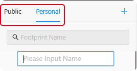
Figure 6-31
6.2.6 Cursor Coordinate Position
Display the current cursor position and grid unit information on the canvas (as shown in Figure 4-61)。
6.2.7 Footprint Toolbar
1.Select
2.Place Pad(Pad Library)
3.Place Custom Pad(Select to place circular, rectangular, oval, and trapezoidal pads)
4.Draw line
5.Draw line arc
6.Draw Circle
7.Draw Rectangle
8.Draw Polygon
8.Place Text
10.Keep out:After clicking this icon, a "Keepout Options" window will pop up (as shown in Figure 6-32). Select the layer where the keepout area will be placed, choose a geometric shape, select to draw or place a rectangle, then click OK. Click on one corner of the keepout rectangle on the canvas, drag the mouse, and click to confirm the opposite corner, completing the placement of the keepout area. After the placement is completed, if you need to modify parameters, select the "Select" option and then click on the keepout area on the canvas; this will cause the "Footprint Properties" window to pop up on the right side of the page (as shown in Figure 6-33), where you can make related parameter adjustments。
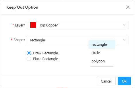
Figure 6-32
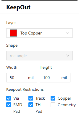
Figure 6-33
11.Measurement(Reference PCB)
6.2.8 Footprint Properties
The interface designed for viewing and editing the attributes of electronic component Footprints. The window for editing information includes details such as the Footprint name, description, Footprint type, manufacturer, and datasheet。
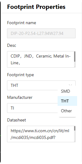
Figure 6-34
6.2.9 Footprint Design Section
The main work area where users carry out the design and editing of electronic component Footprints. Users can create, modify, and adjust the Footprint symbols of components within the canvas area。
6.3 PadStack Editor
Pads are an essential component for connecting electronic parts to the circuit board, and the pad editor is a tool used for editing and customizing the pads on a printed circuit board (PCB)。

Figure 6-35
1、Menu Bar
2、Workbench
3、PadStack Design - Toolbar
4、Switch the editing interface
5、Pad Library
6、Cursor Coordinate Position
7、Pad Toolbar
8、PadStack Properties
9、Layer Selection
10、Pad Design Section
6.3.1 Menu Bar

Figure 6-36
6.3.1.1 File Menu
Save:(Shortcut key Ctrl + S) Save the changes made in the current pad editing session。
6.3.1.2 Edit Menu
Select(Reference PCB)
Undo(Reference SCH)
Redo(Reference SCH)
Origin(Reference PCB)
Move by X,Y(Reference SCH)
6.3.1.3 Tools Menu
Measurement(Reference PCB)
Shortcut Settings(Reference SCH)
6.3.1.4 View Menu
Zoom in(Reference SCH)
Zoom out(Reference SCH)
Zoom fit(Reference SCH)
Unit switch(Reference PCB)
Grid Settings(Reference PCB)
Grid Type(Reference PCB)
6.3.1.5 Place Menu
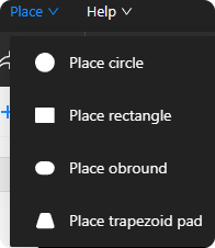
Figure 6-40
Place circle:Select the circular pad tool, adjust the properties of the circular pad, such as stacking, diameter, solder mask clearance, pad type, and position, etc. (as shown in Figure 6-41(a))。
Place rectangle:Select the rectangular pad tool, adjust the properties of the rectangular pad, such as stack layers, width and height, rectangle type, solder mask clearance, pad type, and position, etc. (as shown in Figure 6-41(b))。
Place obround:Select the oval pad tool, adjust the properties of the oval pad, such as stack layers, width and height, solder mask clearance, pad type, and position, etc. (as shown in Figure 6-41(c))。
Place trapezoid pad:Select the trapezoidal pad tool, adjust the properties of the trapezoidal pad, such as stack layers, width and height, trapezoidal increment, trapezoidal axis, solder mask clearance, pad type, and position, etc. (as shown in Figure 6-41(d))。

6.3.2 Workbench
Workbench:After clicking this icon, the page will return to the Workbench。
6.3.3 Pad Design - Toolbar

Figure 6-42
1、Save
2、Undo
3、Redo
4、Move by X,Y
5、Refresh: Refresh the editing interface。
6、Zoom in
7、Zoom out
8、Zoom fit
9、Unit switch
10、Grid Settings
11、Grid Type
12、Measurement
13、Shortcut Settings
6.3.4 Switch the editing interface
Switch the editing interface:Switch between the Symbol editor,Footprint editor, PadStack editor, and Part editor pages。
6.3.5 Pad Library
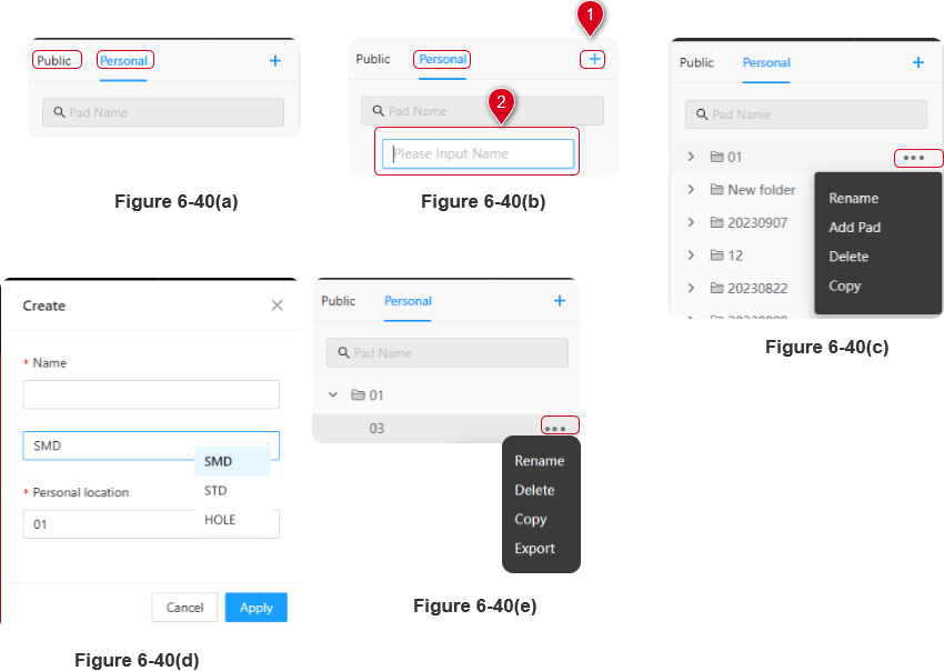
The pad library window is divided into "Public" and "Personal" sections (as shown in Figure 6-43(a)). To create a new pad, you need to first create a Personal library folder for personal use in the "Personal" section。
1、Create Personal Pad Library Folder: As shown in Figure 6-43(b), click the "+" icon at the top right corner of the pad library window, then enter a name in the pop-up window for the new pad library folder。
2、To add a new pad "03" within the newly created Personal pad library folder "01": As shown in Figure 6-43(c), click the "..." next to the folder, select "Add Pad," and a "New" window will appear (as shown in Figure 6-43(d)). In the window, enter the pad name "03," select the pad type, and choose the Personal pad library folder address, then click "Apply." After the addition is complete, it should appear as shown in Figure 6-43(e)。
6.3.6 Cursor Coordinate Position
Display the current cursor location and grid unit information on the canvas (as shown in Figure 4-61)。
8.3.7 Pad Toolbar
Select
Place circle
Place rectangle
Place obround
Place trapezoid pad
6.3.8 PadStack Properties
The interface used for viewing and editing pad attributes. The window editing information includes pad shape, layer selection, solder mask clearance, pad type, and position, etc. (as shown in Figure 6-41)。
6.3.9 Pad Design Section
The main work area where users carry out pad design and editing. Users can create, modify, and adjust pad attributes in the canvas area。
6.4 Part Editor
A tool used to manage and edit the management operations of component symbols and Footprint information

Figure 6-44
1、Workbench:After clicking this icon, the page will redirect back to theWorkbench。
2、Switch the editing interface:Switch between the Symbol editor,Footprint editor, PadStack editor, and Part editor pages。
3、Symbol Library:Select the component symbol that needs to be associated within the window。
4、Symbol/Footprint Match:Click the icon for adding a Footprint located at the bottom right corner of this area,The interface will pop up a "Footprint Library" window. After selecting the target library folder on the left side of the window, choose the component Footprint that needs to be associated on the right side and click OK。
5、Symbol and Footprint Preview:On the left side is the symbol preview, and on the right side is the Footprint preview。
6、Material attributes:Displays the basic information of the component。
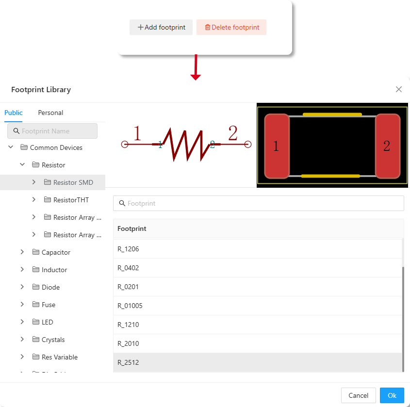
Figure 6-45
After selecting the component symbol and Footprint, click "Apply Changes" at the bottom right corner of the "Symbol/Footprint Match" to use it in the Public library of the SCH (schematic) editor's component symbol selection area。
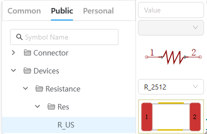
Figure 6-45