
5、PCB Editor
5.1 PCB Design - Main Editing Interface
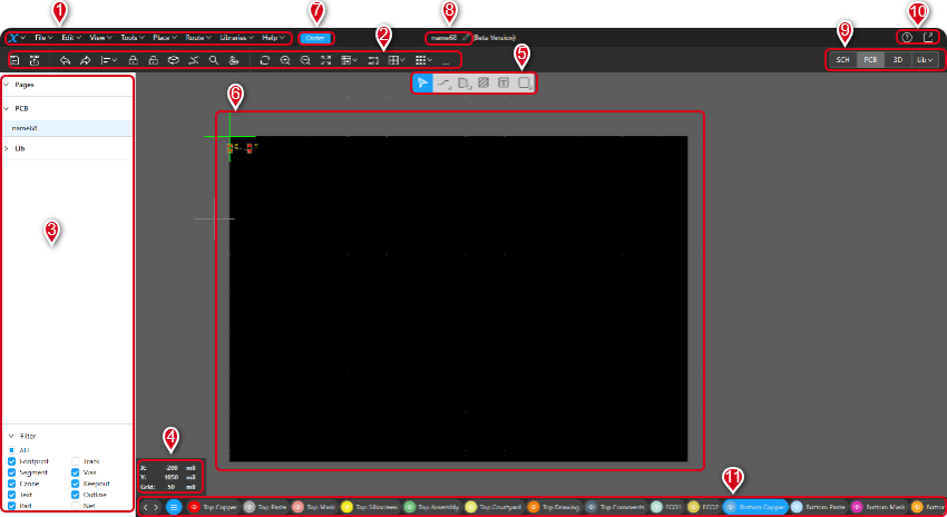
Figure 5-1
① Menu Bar
② ToolBar
③ Project PCB Files and Library Files Selection
④ The same as 6.6
⑤ Quick Access Toolbar
⑥ PCB Layout Area
⑦ Order
⑧ The same as 6.9
⑨ Editor Switching(Refer to 6.10 Editor Switching)
⑩ The same as 6.11
⑪ PCB Layer Selection
5.2 PCB Design - Menu Bar
5.2.1 File Menu
Figure 5-2
Save :Save the current content within the PCB project。(Shortcut Key Ctrl + S) 
Save as:Save a copy of the project file under a new name, requires renaming the project。(Figure 4-4)
Close:Close the currently edited project file and return to the workbench homepag。
Import:Import KiCad, AD, Eagle files。

Export:
1、PCB Fabrication File(Gerber & Drill):The system will directly download the ZIP compressed file containing the PCB manufacturing files。

2、Component Placement(.pos):Select to export the component coordinate file (.POS), and the interface will pop up the 'Export POS' window (Figure 5-3). The file name defaults to the project name, and you can type to modify the name. The output format can be selected as CSV or XLS。
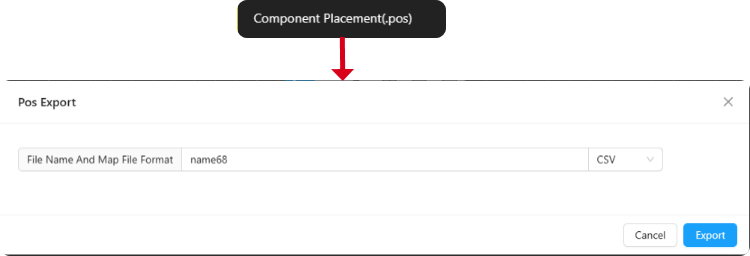
Figure 5-3
3、BOM:Select to export the component BOM (Bill of Materials) list, and the browser will open a new tab named 'PCBX-BOM' (Figure 5-4),The top left corner of the page, from left to right, features the workbench icon (click here to return to the workbench homepage),Save icon (click here to save the changes made to the BOM)、Return to EDA (click here to return from the BOM page to the EDA editing page)、Retrieve component-related information (enter a component keyword to search for the relevant component in the BOM table)。
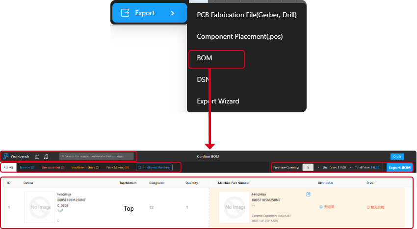
Figure 5-4
PCBX-BOM" tab (Figure 7-4) in the top left corner of the main interface,Can filter to display component types in the BOM table
You can filter to display component types in the BOM table. The top right corner shows the Purchase Quantity, Unit Price, and Total Price (the single set price is the price per set for components that have been successfully matched in the BOM table, with the component quotations sourced from )。
The main interface of the "PCBX-BOM" tab, on the left half, displays information that includes the BOM list:ID、Device(Preview image, Manufacturer, Part Number,Footprint, and Value)、Top/Bottom(Component Layer)、Designator、Quantity;The right half displays information that includes: Matched Part Number(Preview image, Manufacturer, Part Number,Footprint, and Value)、Distributor(Main source eecart )、Price(Unit price and Total price)。
Click the icon in the Distributor column of the BOM table,The page will open the "Material Matching" window (Figure 7-5)。You can select the corresponding material from the matched materials list in the bottom right corner of the window. By moving the cursor to the corresponding device row and clicking, you can choose the appropriate material,Click on the icon in the corresponding part number column to open the datasheet for the respective part number。
You can also find corresponding materials on the left side of the "Material Matching" window according to the device type, or enter material-related information in the search box at the top of the window to perform a search (supporting search for material information such as part number, category, manufacturer, distributor, etc.)。

Figure 5-5
Click on the option in the "PCBX-BOM" tab (Figure 5-4),The page will pop up an "Export BOM" window (Figure 5-6),The BOM can be viewed in the window:ID、Part number、Manufacturer、Top/Bottom、Designator、Value、Footprint、QtyIn the top right corner of the window, you can choose the BOM table display type to be "Consolidated View" (where components with the same value are combined into the same row),and "Individual View" (where each component reference designator is displayed on a separate line). Enter the BOM table filename (default is the project filename), select the output format (CSV or XLS options available), and click on Export to complete the export of the materials BOM table。
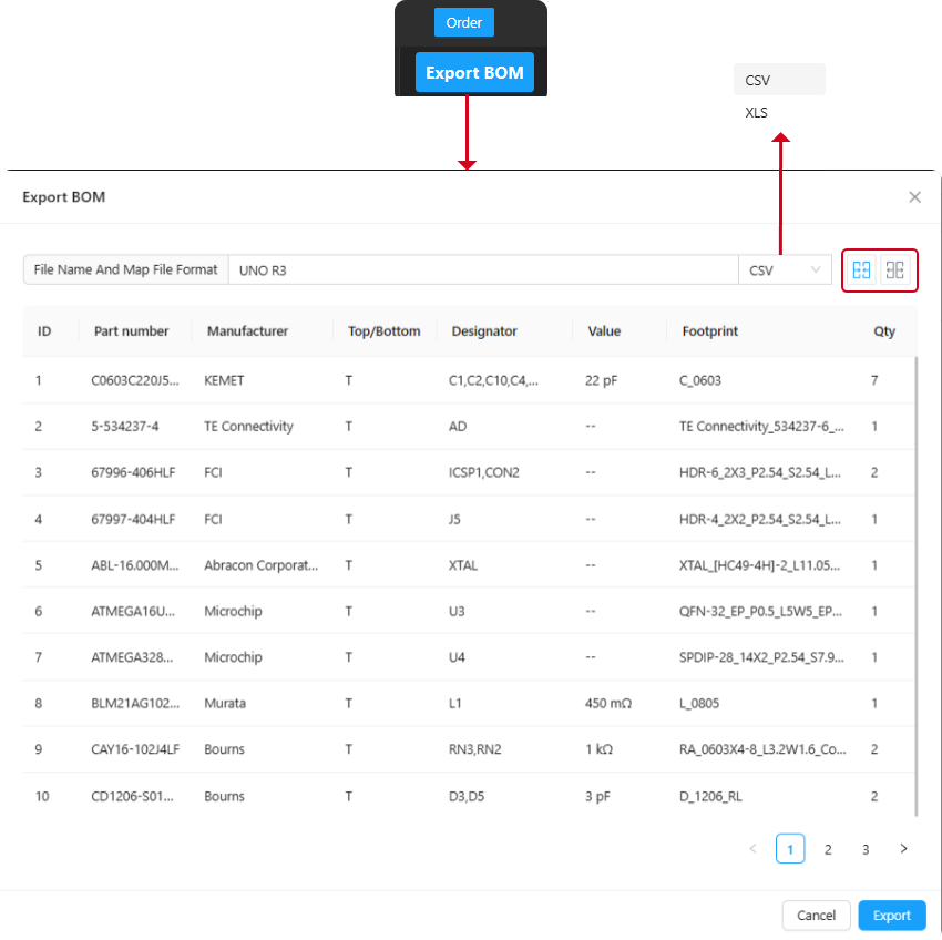
Figure 5-6
4、DSN:Select the export option,The system will export the .DSN format file。
5、Export Wzard:Select the export wizard option,The page will pop up the "Export Wizard" window (Figure 5-7), where you can perform simultaneous export operations for multiple file types, including the project schematic, project PCB, project symbol library, project footprint library, and project BOM (Bill of Materials) table。
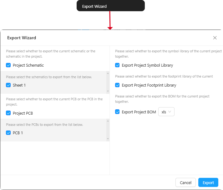
Figure 5-7
 5.2.2 Edit Menu

Figure 5-8
1、Select :Select a feature; the selection options include six types of selection: Select, Touching Line, Same Connect Network,Connect Objects,Component Connectiol, and Component Nets。
(1)Select:Basic selection tool, which allows designers to click, drag, or create a selection box to choose components, wires, and other design elements. The selection box can be categorized into rightward selection or leftward selection:
With rightward selection, the frame color appears green, and only elements that are completely inside the selection box are selected (full containment);
With leftward selection, the frame color is gray, and elements are selected as long as part of them is within the selection box (partial containment);

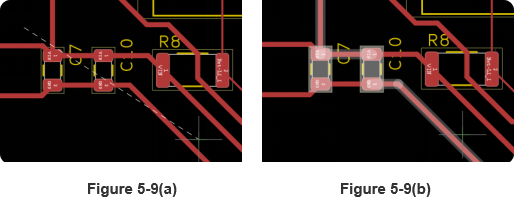
(2)Touching Line:This method of selection is particularly suitable for situations where multiple elements need to be selected at once. Designers first use the cursor position (click the left mouse button after determining the starting point) to select the starting point of the line selection, then move the cursor position (click the left mouse button again after determining the end point) to select the end point of the line selection。
During the line selection process, after the starting point is determined and the cursor is moved, a (dashed) straight line is automatically generated between the starting point and the cursor (as shown in Figure 5-9(a)). Any elements that this line passes through will be selected (as shown in Figure 5-9(b)).
(3)Connect Network:Select related components quickly based on their electrical network connections. In PCB design, components are interconnected through electrical networks. The 'Same Net Connections' selection function can be used to quickly select all relevant components on the same network, such as the same power supply line, the same signal line, etc. It is primarily used for operations involving the entire electrical network. For example, as shown in Figure 5-10, after selecting the 'Same Net Connections' function, move the cursor to the VIN network at pin 1 of the resistor R8 and click the left mouse button to confirm the selection. Then all the elements related to the VIN network on the PCB will be selected and highlighted (even if they are not actually connected, as long as they are on the same network, they will be selected)。

Figure 5-10
(4)Connect Objects:This functionality is used to select all other elements that are connected to a chosen component, making it easier to select and manipulate all the components of a specific connection at once. When designers need to inspect or edit all elements on a particular signal or power pathway, this tool can be quite helpful. It is mainly used for operations that involve the direct connections of specific elements。For example, as shown in Figure 5-11, after choosing the 'Element Connection Objects' feature, moving the cursor to the VIN network on pin 1 of the R8 resistor and clicking the left mouse button to confirm the selection will select and highlight all the VIN network-related elements that are connected through completed routing operations to pin 1 of R8 (only the same networks that are connected through completed routing will be selected; the VIN network on pin 1 of capacitor C10 on the left, which has not yet been routed, will not be selected)。
Figure 5-11
(5)Component Connections:Using the 'Component Connection Selection' feature allows selection of all elements that are directly electrically connected to a chosen component, including wires and other devices. This tool enables designers to easily visualize and modify the connections of a specific device on the PCB, thus improving both the efficiency and accuracy of the design process.
For example, as shown in Figure 5-12, after selecting the 'Component Connection' function, moving the cursor over the resistor R8 and clicking the left mouse button to confirm the selection will highlight the network elements that are directly connected to both ends of R8 — the VIN network and the Net-L1_1 network that have completed routing with R8 will be selected and highlighted。
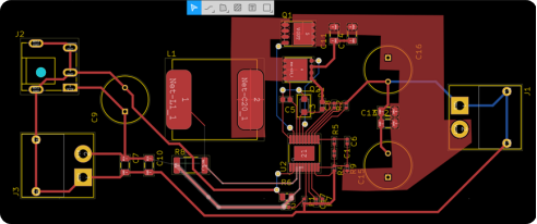
Figure 5-12
(6)Component Nets:Using the 'Component Net Selection' tool, designers can select all elements that are connected on the same electrical network with the selected component, including wires, other components, etc. This feature allows designers to efficiently review and edit all the devices on a specific electrical network on the PCB, enhancing the design's efficiency and accuracy.
For example, as illustrated in Figure 5-13, after selecting the 'Component Net Selection' function, moving the cursor to resistor R8 and clicking the left mouse button to confirm will highlight both of the networks at the ends of R8 — the entire VIN network and the Net-L1_1 network within the PCB file will be selected and displayed in a highlighted state。
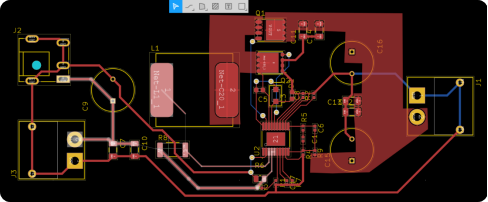
Figure 5-13
2、Find 8 Replace, to find and replace relevant elements in the PCB file, the content to be found can be optioned as reference designator, part number, text, net, and all of the above。(Shortcut key Ctrl + F)
The content for replacement can be optioned as reference designator, text, net, and all of the above。
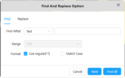
Figure 5-14

Figure 5-15
3、Rotate the selected component footprint, rotate right (shortcut key R), rotate left (shortcut key E)。
4、Delete the selected element, or use the keyboard Delete key for the same function。
5、Copy the selected elements。(Shortcut key Ctrl + C)
6、Paste the elements copied last time. When pasting components, the reference designator will be reset。(Shortcut key Ctrl + V)
7、Mirror flip the selected component footprint along the X (horizontal) axis. (Shortcut key Shift + Y), mirror flip the selected component footprint along the Y (vertical) axis。(Shortcut key Shift + X)
8、Flip the component。 (Shortcut key F)
9、Undo Refer to the same function in the SCH Editor。
10、Align RedoRefer to the same function in the SCH Editor。
11、Lock Refer to the same function in the SCH Editor。
12、Unlock Refer to the same function in the SCH Editor。
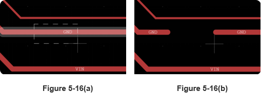
13、Slice Tracks:After selecting the 'Break Wire' function, use the cursor to create a selection box around the area of the trace that needs to be broken to perform the breaking operation (as shown in Figure 5-16)。
14、Origin:The setting and resetting of the origin. By choosing the option to set theorigin (shortcut key Ctrl + Shift + X) and then clicking on a position in the PCBlayout, you can manually set the origin. By selecting the option to reset the originshortcut key Ctrl + Shift + C), the origin will be restored to the software's default position。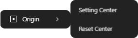
5.2.3 View Menu
1、Zoom In: Refer to the same function in the SCH Editor。
2、Zoom Out: Refer to the same function in the SCH Editor。
3、Zoom Fit: Refer to the same function in the SCH Editor。
4、Show/Hide Rats:In the PCB editing environment, a rat's nest (Ratsnest) consists of virtual lines connecting unconnected pins, used to indicate the connections on the PCB. In the PCB view, you can choose to show or hide these rat's nest lines to more clearly view the circuit board's connections。
(1)Show all:Click "Show All" to display all unrouted rat's nest connections on the canvas, including those that were previously hidden (as shown in Figure 5-18). The 'Show All Rat's Nest' feature helps designers better understand the connections on the circuit board, especially during debugging and optimization in the design phase。

Figure 5-18
(2)Show net:Display the rat's nest lines associated with a specific network (Net). Click "Show Net," and then click on an object that belongs to the network to display all unrouted rat's nest connections within the same network. As shown in Figure 5-19, after clicking "Show Net," selecting the VIN network on pin 1 of resistor R8 will display all VIN network rat's nest lines on the PCB editing page。
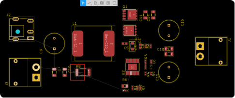
Figure 5-19
(3)Show area:Within the selection area, show the rat's nest lines for all networks. In the PCB editing view, drag to draw a selection box around an area to choose the networks whose rat's nest lines you wish to display. (As shown in Figure 5-20)。
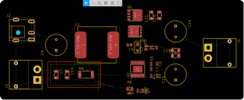
Figure 5-20
(4)Hide all:Opposite in logic to "Show All。
Figure 5-21
(5)Hide Net:Opposite in logic to "Show Net.”。
Figure 5-22
(6)Hide Area:Opposite in logic to "Show Area.”。

Figure 5-23
5、Grid Settings:Refer to the same function in the SCH Editor。
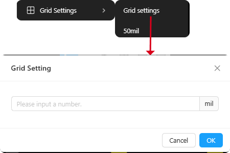
Figure 5-25
6、Grid Type:Refer to the same function in the SCH Editor。
7、Unit Switch:Refer to the same function in the SCH Editor。
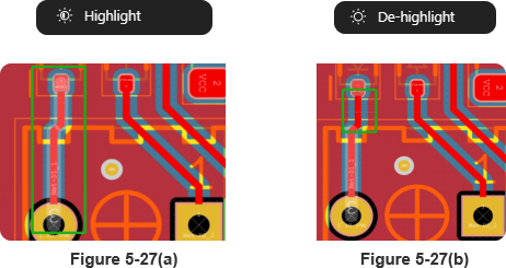
8、Highlight or De-highlight: Refer to the same function in the SCH Editor。Complete the selection with a left mouse click.Figure 5-27(a) is for selection highlighting, and Figure 5-27(b) is for canceling highlighting
9、Flip Board:The "Flip Board" function is used to change the orientation of the circuit board, making it easier to lay out and adjust the position of components. After executing the flip command, the entire board is flipped. The board view undergoes a horizontal flip (left to right flip), switching from the original "top view" to a "bottom view." Figure 5-28(a) shows the view of the PCB before flipping (top view), and Figure 5-28(b) shows the view of the PCB after flipping (bottom view).

Figure 5-28(a)
Figure 5-28(b)
10、Full Screen Cross Cursor:Refer to the same function in the SCH Editor。
5.2.4 Tools Menu
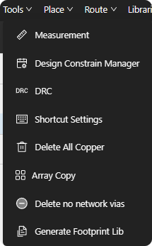
Figure 5-30
 1、Measurement: The measurement function is a very critical tool for ensuring the accuracy of the circuit board design. After selecting the "Measurement" function from the "Tools" menu, click the first point to be measured, then click the second point to determine the distance between them. As shown in Figure 5-31, measure the distance between the two pins of capacitor C9。(Shortcut key Ctrl + M)
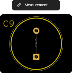
Figure 5-31
2、Design Constrain Manager:Through the Design Rule Manager, designers are able to identify potential issues at an early stage of design, improving the quality of the design and reducing errors and costs during manufacturing and testing. It is one of the indispensable tools in PCB design。(Shortcut key Ctrl + Shift + R)
From the "Tools" menu, select the "Design Rule Manager" function to open the "Design Rule Manager" interface。
(1)Electrical- Clearance: In the Design Rule Manager interface, left-click on "Spacing" under the DRC (Design Rule Checking) rules (as shown in Figure 5-32) to change the electrical clearance rules between traces, surface pads, through-hole pads, vias, copper areas, and geometric shapes。
By setting these rules, it is possible to ensure that there is sufficient space between various elements of the PCB to meet design requirements, manufacturing standards, and reliability requirements. Note that in the Design Rule Manager, different rules can be created and set for different types of elements to meet specific design needs。

Figure 5-32
(2)Routing-Width:Width rules settings include minimum width, preferred width, and maximum width (as shown in Figure 5-33). Width rules are used to define the range of widths for traces on a circuit board to ensure they meet electrical performance, manufacturability, and reliability requirements。

Figure 5-33
(3)Routing-Routing Via:The overhole rule setting involves the inner and outer diameter of the holes (see Figure 5-34) to ensure that these holes meet the electrical performance, manufacturability and reliability requirements of the project.
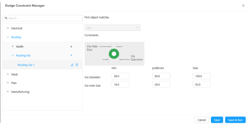
Figure 5-34
(4)Mask - Solder Mask Expansion:Used to define the distance between the solder mask layer and the copper layer (as shown in Figure 5-35), to ensure that during manufacturing, the solder mask is not too close to the copper layer, avoiding potential manufacturing issues such as insufficient solder mask coverage, which can cause short circuits, etc. This helps improve the manufacturability and reliability of the PCB. You can change the expansion size of the top and bottom layer solder mask。
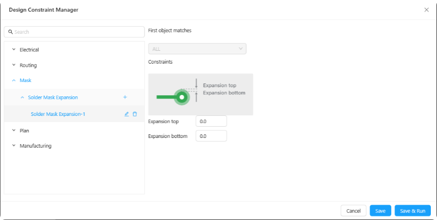
Figure 5-35
(5)Plan - Polygon connect style:The copper pour connection style rules settings involve different connection methods, including solid and crosshatch (as shown in Figure 5-36). It is used to define the way copper pours connect to pads and vias to satisfy electrical performance and manufacturing requirements。
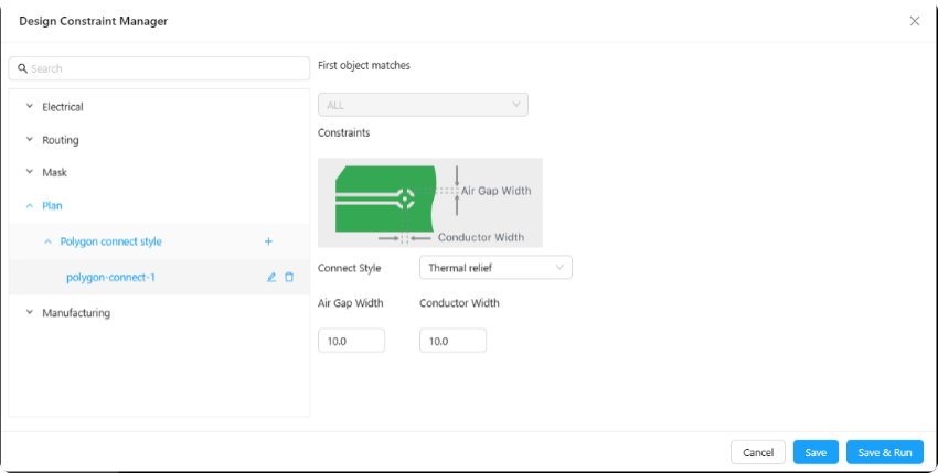
Figure 5-36
(6)Manufacturing - Minimum Annular Ring:Used to define the minimum size of an annular ring by setting the minimum annular ring radius (as shown in Figure 5-37)。

Figure 5-37
(7)Manufacturing - Min Solder Mask Sliver:Used to define the minimum spacing between solder mask layers (as shown in Figure 5-38). By setting the minimum solder mask spacing rules, it ensures that the solder mask can be correctly applied during the manufacturing process, preventing manufacturing issues caused by insufficient or excessive solder mask coverage。
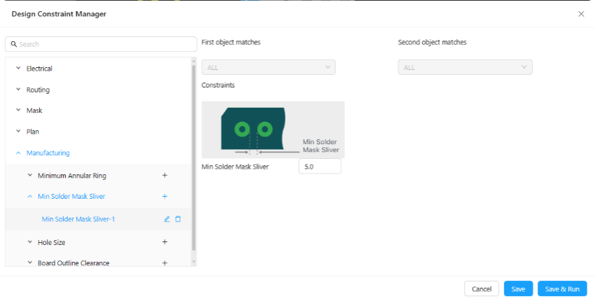
Figure 5-38
(8)Manufacturing - Hole Size:Used to define the minimum size for drill holes on the PCB that are used to connect different layers (as shown in Figure 5-39). By setting the minimum drill size rules, it ensures that the holes drilled to connect different layers meet design and manufacturing requirements. This helps to avoid potential issues during manufacturing, such as drill holes being too small to pass through traces or too large, resulting in unreliable electrical connections。
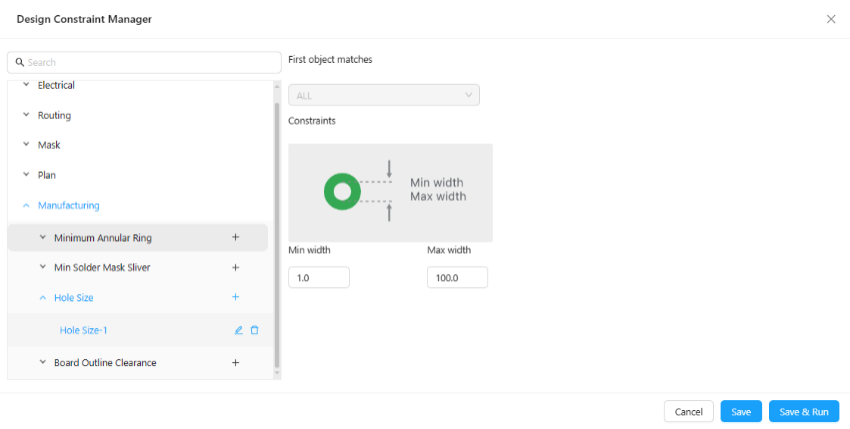
Figure 5-39
(9)Manufacturing - Board Outline Clearance:The contour clearance rules settings involve defining the clearance between different elements to ensure the manufacturability and electrical performance of the design. It includes clearance rules between the board outline and traces, board outline and surface pads, board outline and through-hole pads, board outline and vias, board outline and copper areas, board outline and text, as well as the board outline and geometric shapes。

Figure 5-40
3、DRC(Design Rule Check):DRC is an important feature used to verify if design rules comply with manufacturing requirements. DRC helps ensure that the PCB design is compliant, manufacturable, and reliable at the manufacturing level. After running the DRC function, a report window will be displayed at the bottom of the PCB editing interface, which primarily shows information such as error type, count, constraint name, and location (as shown in Figure 5-41). DRC checks for a range of error types, which include the following 11 categories:
①Un-Routed Net Constraint:In the circuit, there are nets that are not connected to any other components or to the power/ground。
②Net Antennae:There are leads with unconnected ends in the circuit; that is, a net has a single-ended connection resembling an antenna (one end is not connected to any electrical part) and it has not been set with an antenna property, thus it causes an error. This can produce an antenna effect and interfere with other components。
③Pad And Pad Overlap:There is an overlap between pads。
④Clearance Constraint:The distance between components, traces, or other design elements does not meet the specified minimum spacing requirements。
⑤Width Constraint:The width of the traces does not comply with the specified minimum or maximum width requirements。
⑥Via Constraint:The specifications of vias (through-holes or blind vias) in the design do not meet manufacturing requirements。
⑦Hole Size Constraint:The dimensions of vias in the design do not meet the specified requirements。
⑧Minimum Solder Mask Sliver:The distance from the solder mask layer to the traces or components does not meet the specified minimum requirements。
⑨AnnularRing Constraint:The size of the annular rings does not meet the specified minimum requirements。
⑩Min Solder Mask Sliver:The minimum spacing between solder mask layers or from a solder mask layer to other elements does not meet the specified requirements。
⑪Outline Constraint:The distance between geometric shapes (which may be drawn shapes or patterns) in the design does not meet the specified minimum spacing requirements。

Figure 5-41
4、Shortcut Settings:Refer to the Shortcut Key Settings content in the Tools Menu of the circuit design, section 4.3.4。
5、Delete All Copper:Selecting the "Delete All Copper" function will remove all copper pours on the canvas, including both connected and unconnected copper pours。(Shortcut key Shift + M) 
6、Array Copy:Refer to the same function in the SCH Editor。
 7、Delete no network vias:If there are unconnected vias in the PCB layout, clicking the "Delete no network vias" function will remove all the unconnected vias (as shown in Figure 5-43)。
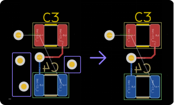
Figure 5-43
8、Generate Symbol Lib:The same logic as "Generate Symbol Lib" in the SCH。

Figure 5-44
After entering the library name and clicking "OK" or "Generate and Enter," you can see the information of the just generated footprint library in the Personal library of the footprint editor once the generation of the footprint library is completed (as shown in Figure 5-45)。
Figure 5-45
 5.2.5 Place Menu
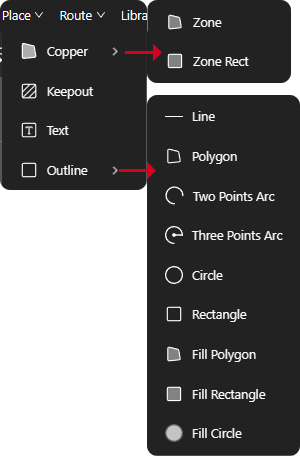
Figure 5-46
1、Copper:It is used to create copper fill areas in PCB layouts to provide good electrical performance, connectivity, and heat dissipation. Refer to the following specific steps for operation:
(1)Select the Copper Pour function:Choose the polygon copper pour or rectangular copper pour (as shown in Figure 5-47), and draw the copper pour area on the canvas;
(2)After drawing is complete, press the ESC key to return to the selection mode, and then select the copper pour area that is in selection mode;
(3)Change the copper pour network in the properties panel on the right, and use the shortcut keys (X: Repour current layer; Z: Repour selected copper pour; Shift+M: Delete all copper pours; Shift+B: Repour all copper pours.) to repour the copper pour area (as shown in Figure 5-48)。
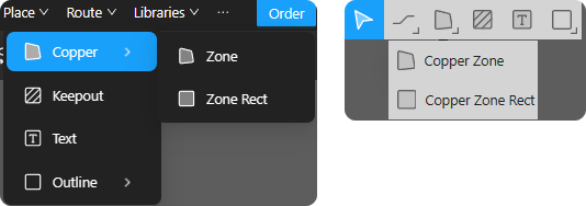
Figure 5-47
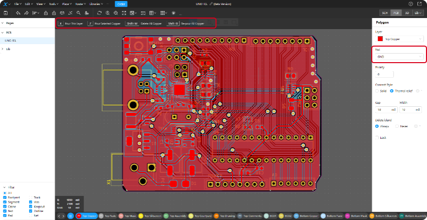
Figure 5-48
 2、Polygon pour cutout:Trim the already laid copper layers to fit the needs of specific areas or shapes. This function allows designers to precisely define the shape of the copper layers to meet the requirements of the circuit design. After selecting the "Copper Pour Trim" function (note: you need to select the copper pour to be modified before choosing the "Copper Pour Trim" option), the page will pop up a "Copper Pour Cut Options" window, with the shape selectable as either rectangle or polygon. As shown in Figure 5-50(a) rectangular copper pour trim operation was performed on the SW1 Footprint area, Figure 7-50(a) is before the operation, and Figure 5-50(b) is after the operation。

Figure 5-49
Note: After completing the drawing of the trim shape, press the ESC key to return to selection mode, and then perform the copper pour update operation。

3、Keepout:The purpose of a keep-out area is to prevent specific regions on the circuit board from having traces routed, copper poured, or components placed over them, to meet certain requirements of the circuit design. Refer to the following specific steps for operation:
(1)Select the Keep-Out Area function option:From the "Place" menu, select the "KeepOut" function, or by clicking on the "KeepOut" icon on the left toolbar(Figure5-51)。
(2)Draw the Keep-Out Area:Create a keep-out area on the PCB canvas using the "Place" menu or the "Keep-Out" function in the left toolbar to draw the shape of the area where you want to prohibit components or copper from being placed. As shown in Figure 5-52 at location ①, a keep-out area is drawn around the Power1 component footprint。
(3)In the properties panel on the right side of the PCB editing interface, you can select the objects that are not allowed to be placed in the keep-out area (as shown at location ② in Figure 5-52)。

Figure 5-51
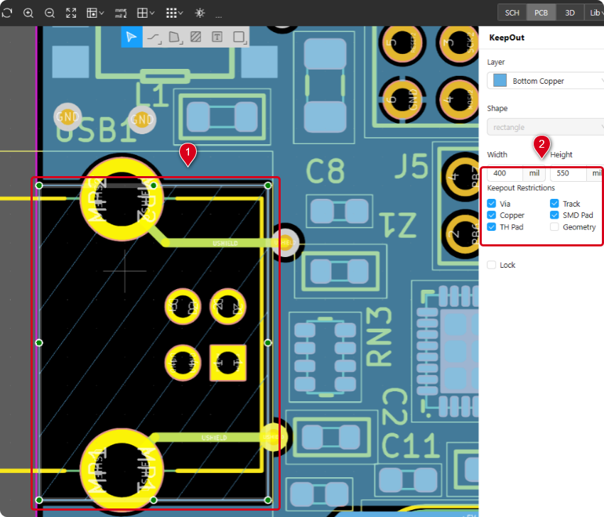
Figure 5-52
4、Text: The same as the text placement function in the SCH。
5、Drawing Tools:Used to create lines, polygons, arcs, circles, rectangles, and perform fill operations (as shown in Figure 7-54)。
①Line:Select the Line Tool, click the starting position, drag the mouse and click the end position; adjust the line's attributes, such as line width, layer stacking, etc。
②Polygon:Select the Polygon Tool, click on each vertex of the polygon in turn; adjust the properties of the polygon, such as line width, layer stacking, etc.
③Two Points Arc:Select the Two-Point Arc Tool, click on the starting and ending points of the arc; adjust the properties of the arc, such as line width, layer stacking, radius, angle, etc。
④Three Points Arc:Select the Three-Point Arc Tool, click on the starting point, middle point, and ending point of the arc; adjust the properties of the arc, such as line width, layer stacking, radius, angle, etc。
⑤Circle:Select the Circle Tool, click on the center of the circle, drag the mouse and click the boundary of the circle; adjust the properties of the circle, such as radius, line width, layer stacking, etc。
⑥Rectangle:Select the Rectangle Tool, click one corner of the rectangle, drag the mouse and click the opposite corner; adjust the properties of the rectangle, such as line width, layer stacking, rectangle type (selectable from three types: rectangle, chamfered rectangle, rounded rectangle), width, height, etc。
⑦Fill Polygon:Select the Fill Polygon Tool, click on each vertex of the polygon in sequence; after completion, select the layer on which the fill is located in the properties window。
⑧Fill Rectangle:Select the Fill Rectangle Tool, click on one corner of the rectangle, drag the mouse and click the opposite corner; after completion, adjust the properties of the filled rectangle such as layer stacking, rectangle type (selectable from three types: rectangle, chamfered rectangle, round-cornered rectangle), width, height, etc。
⑨Fill Circle:Select the Fill Circle Tool, click on the center of the circle, drag the mouse and click on the boundary of the circle; after completion, the properties of the filled circle, such as the layer stacking, radius, etc., can be adjusted。

Figure 5-54
5.2.6 Route Menu
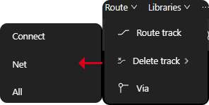
Figure 5-55
1、Route:Select the Wire Tool (shortcut key W), or choose it from the "Wire" menu, or by clicking on the "Wire" icon on the left toolbar to select the "Wire" tool (as shown in Figure 5-56)。
When using the "Wire" function, clicking a pad will allow you to connect other pads on the same network by drawing wires from the selected pad (as shown at location ① in Figure 5-57). If you want to change related properties while using the "Wire" function, you can press the "Tab" key, and a Wire Properties window will pop up on the right side of the editing page, where you can adjust properties such as layer stacking (selectable between top copper or bottom copper), corner style (options of arc or direct, with angles of 45° or 90°), avoid (selectable from route around, push, or ignore), line width, and other properties (as shown at location ② in Figure 5-57)。
Note: The "Arc" corner style option has not yet been developed!

Figure 5-56
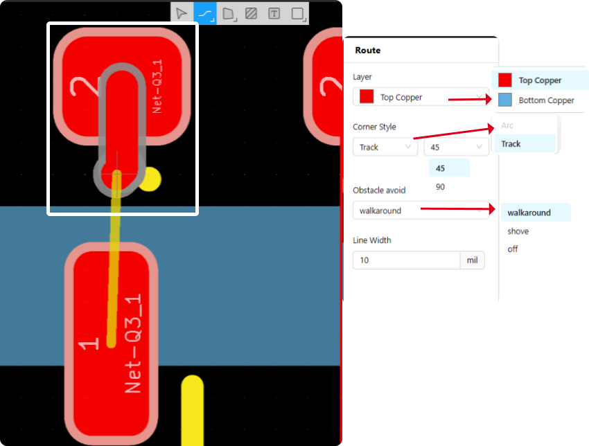
Figure 5-57
2、Delete track:Deletion types include three sub-options: Connect, Net, and All。
(1)Delete Wire Connection:As shown in Figure 5-58, the "Delete Wire - Connection" operation will be performed on the Net-C1_2 network in the diagram. From Figure 5-59, you can see that the selected wire branch is deleted after the "Delete Wire - Connection" operation。
Figure 5-58

Figure 5-59
(2)Delete Wire Net:As shown in Figure 5-58, the "Delete Wire - Net" operation will be performed on the Net-C1_2 network in the diagram. From Figure 5-60, you can see that the wire segments of the same network are deleted after the "Delete Wire - Net" operation。
Figure 5-60
(3)Delete All Wires:After selecting this operation, all the wires on the entire PCB will be deleted (as shown in Figure 5-61)。
Figure 5-61
3、Via:Via is used to achieve electrical connections between different layers. Vias can be categorized into through-holes, blind vias, buried vias, as well as non-plated holes (NPTH)。
The Via function can be selected using the shortcut key V, or chosen from the "Wire" menu, or by clicking on the "Via" icon in the left toolbar to select the "Via" tool (as shown in Figure 5-62)。
After selecting the "Via" function, choose the location on the canvas where you want to place the via (as shown at location ① in Figure 5-63). If you want to change related properties while using the "Via" function, you can press the "Tab" key, and a Via Properties window will pop up on the right side of the editing page, where you can adjust properties such as the via net, via diameter, via drill size, via type (options of through-hole, blind vias, buried vias, and non-plated holes), as well as start layer and end layer, among others (as shown at location ② in Figure 5-63)。
(1)Through-Hole Via: A through-hole is a type of via that completely penetrates from one side of a PCB to the other. They go through all layers of the board, providing electrical connections. In design software, you typically have a specific tool that you can use to place through-holes。
(2)Blind Via: A blind via is a type of via that connects only one of the outer layers to an inner layer. They do not penetrate through the entire board but instead connect to one or more internal layers. In design software, you need to specify the layers that the blind via connects and the location of the via。
(3)Buried Via: A buried via is a type of via that is completely located within the interior of a PCB and does not connect to any of the outer layers. They are used to establish connections within the interior of multilayer boards. In design software, you need to place buried vias between internal layers and ensure that they properly connect。
(4)Non-conductive Via: Non-plated holes (NPTH) are non-conductive and are mainly used for mechanical purposes such as alignment, mounting, or providing clearance for a part that passes through the hole. They are not used for establishing electrical connections and do not have conductive plating along the inner surface of the hole. In design software, you may need to specify certain holes as non-plated and consider their mechanical purpose in the stack-up design。
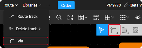
Figure 5-62
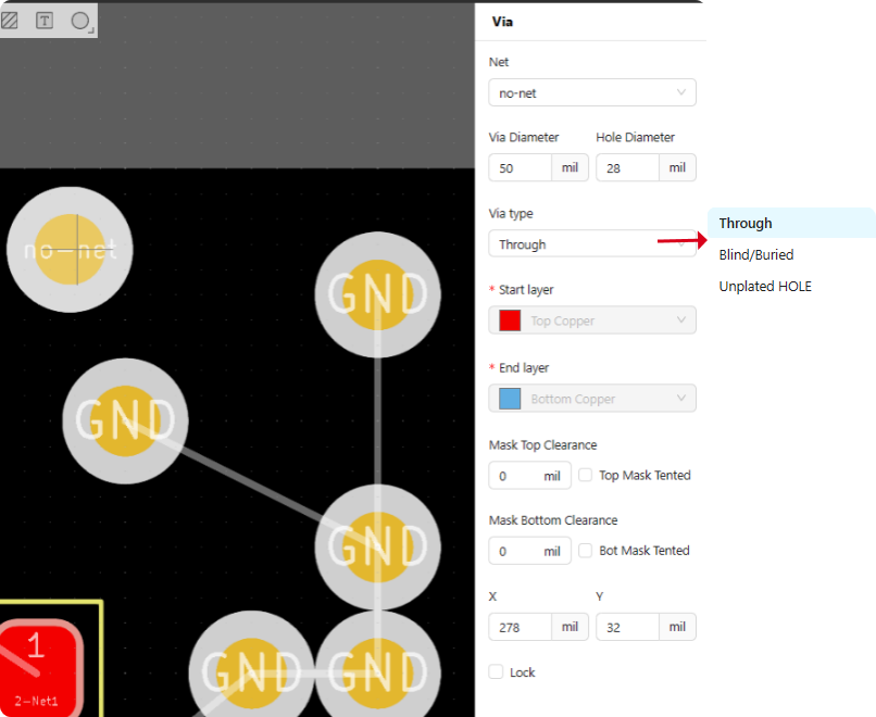
Figure 5-63
5.3 PCB Design - Toolbar
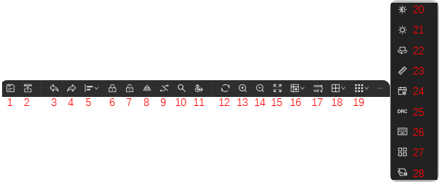
Figure 5-64
1、Save
2、BOM
3、Undo
4、Redo
5、Align
6、Lock
7、Unlock
8、Mirror
9、Slice Tracks
10、Find & Replace
11、Move by XY
12、Refresh: Refresh the editing interface。
13、Zoom In
14、Zoom Out
15、Zoom Fit
16、Show/Hide Rats
17、Unit Switch
18、Grid Settings
19、Grid Type
20、Highlight
21、De-highlight
22、Flip board
23、Measurement
24、Design Constrain Manager
25、DRC
26、Shortcut Settings
27、Array Copy
28、Layers Editor
Layer Stack Manager is used for managing and configuring the stack-up information in PCB design. Through the Layer Stack Manager, designers can define and control the various layers of the PCB, the stack order between the 
 layers, and the properties of each layer。Clicking on the Layer Stack Manager icon in the top toolbar will open the Layer Stack Manager interface。
The Layers Editor interface is divided into two parts: "Physical Stacking" and "Layer Management."
(1)Physical Stacking:In the "Physical Stacking" section of the "Layers Editor" interface, the number of layers can be adjusted、Board Thickness、Layer、Name、Type、Material、Thickness、Color、Epsilon R、Loss Tan and other attribute parameters (as shown in Figure 7-65)。
①Copper layers:Refers to the number of layers of the PCB, that is, the physical levels of the board. Through the Layer Stack Manager, you can define and configure the number of layers in the PCB to meet the electrical and mechanical requirements of the design. The number of layers can be set to an even number between 2-16 layers。
②Board Thickness:Represents the overall thickness of the PCB board. Through the Layer Stack Manager, you can specify the total thickness of the board and consider the mechanical and electrical characteristics in the design. The board thickness can be set (in even numbers) from 0.4 to 3.2mm。
③ Layer:Refers to the order of layers within the PCB。
④Layer Name: Each layer has an identifiable name for easy recognition。
⑤Type: The type of physical stackup。
⑥Material: The material of PCB layers refers to the substrate material used for that layer. Through the Layer Stack Manager, different materials can be selected (currently, FR-4 is supported as a choice)。
⑦Thickness: The physical thickness can be specified for each layer of the stackup。
⑧Color: Refers to the actual color of the manufactured circuit board, specifically the color of the top and bottom layer silkscreen (options include black or white) and the top and bottom layer solder mask (options include green, blue, black, red, yellow, white)。
⑨Epsilon R and Loss Tan: Describes the electrical characteristics of alayer. The dielectric constant represents the insulating performance ofthe layer, and the loss tangent is related to energy loss during signaltransmission。

Figure 5-65
(2)Layer Management:In the "Layer Management" section of the "Layers Editor" interface, you can adjust attributes such as the number of layers, color, transparency, stackup names, and other parameters (as shown in Figure 5-66).
①Copper layers:The same as in the "Physical Stacking."。
②Color: Through the Layer Stack Manager, a unique color can be selected for each layer. This helps to distinguish between different layers in the design interface, enhancing the visualization effect。
③Transparency: The transparency of the layers can be adjusted for clearer viewing between elements of different layers. The transparency setting allows you to adjust the visibility of the layers。
④Layer Naming: Define an easily recognizable name for each layer stack. This name is commonly used during the design process to reference and locate the layer stack。

Figure 5-66
5.4 PCB Toolbar

Figure 5-67
1、Select
2、Place Via/Track
3、Place Copper
4、Place Keepout
5、Place Text
6、Drawing Tools
5.5 PCB Layer Selection
As shown in Figure 5-68, there is a layer selection area at the bottom of the PCB editing page, used to manage and select the currently active layer. This is an important user interface element; clicking the "little eye" icon on the left side of the corresponding layer can control the layers that are visible in the design. Detailed layer stack parameters can also be set in the Layers Editor。

Figure 5-68